Search
Search Results
-
The Electrical Characteristics of 1200 V Trench Gate MOSFET Based on SiC
This research was carried out experiments with changing processes and design parameters to optimally design a SiC-based 1200 V power MOSFET, and...

-
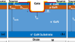
4.87 kV SiC MOSFET Using HfSiOx/SiO2 Gate Dielectrics Combined with PN Pillars
A novel structure of a silicon carbide (SiC) double-trench metal oxide semiconductor field-effect transistor (DTMOSFET) is proposed using a hafnium...

-
Vertical GaN Reverse Trench-Gate Power MOSFET and DC-DC Converter
A vertical GaN reverse trench-gate power MOSFET (RT-MOSFET) device is proposed. This Vertical RT-MOSFET features the negative incline of...
-
1.3 kV Vertical GaN-Based Trench MOSFETs on 4-Inch Free Standing GaN Wafer
In this work, a vertical gallium nitride (GaN)-based trench MOSFET on 4-inch free-standing GaN substrate is presented with threshold voltage of...

-
Snapback-Free Reverse-Conducting SOI LIGBT with an Integrated Self-Biased MOSFET
A novel snapback-free RC-LIGBT with integrated self-biased N-MOSFET is proposed and investigated by simulation. The device features an integrated...

-
Inversion-type p-channel diamond MOSFET issues
This article reviews the state of the art in inversion-type p-channel diamond MOSFETs. We successfully developed the world’s first inversion-channel...

-
An Assessment of Step Patterned Gate Oxide Superjunction Trench MOSFET for Potential Benefits
A 600 V-class step patterned gate oxide trench (SPGOT) superjunction vertical device incorporating gate engineering is proposed in this paper. An
... -
A Study of the Performance of an N-Channel MOSFET Under Gamma Radiation as a Dosimeter
This paper is devoted to the effect of gamma radiation on commercial IRFP250 N -channel metal oxide semiconductor field effect transistors (MOSFETs)...
-
Superior Impact Ionization Rate in Deep Gate LDMOS Devices to Improve the Figure of Merit and Lattice Temperature
This paper introduces a deep gate lateral double-diffused MOSFET (LDMOS) structure. The proposed LDMOS is a superior impact ionization rate...

-
Atomic Layer Etching Applications in Nano-Semiconductor Device Fabrication
These days, the process of plasma etching is exhibited in various forms, including the reactive ion etching (RIE) method. Not only memory device but...

-
Influence of Structural Parameters on the Behavior of an Asymmetric Linearly Graded Workfunction Trapezoidal Gate SOI MOSFET
This paper presents a dual metal trapezoidal recessed channel metal oxide semiconductor field effect transistor (MOSFET) embedded with asymmetric...
-
Charge Plasma TFET-Based Label-Free Biosensor for Healthcare Application
Because of the capability of biosensing technology in the medical field, environmental monitoring, and security applications, field-effect...
-
A Detailed Review on Growth and Evolution of TFET Biosensor for Biosensing Application
Researchers around the world identified the importance of biosensors to detect biological life. The growth of efficient technology to aid the...
-
Accomplishing Low-Power Consumption with TFET
Low-power electronics utilize the least amount of energy possible to perform their intended function. Power management, energy-efficient design, and...
-
Total Ionization Dose (TID) Effects on 2D MOS Devices
Electronics and Electricals devices are used in radiations environments for space applications. Radiation has immense potential to disturb the basic...

-
Analysis of Electrical Characteristics of Shielded Gate Power MOSFET According to Design and Process Parameters
This paper designed a structure of the shielded trench gate power MOSFET device, which has been applied to small capacity (less than or equal to...

-
Nanosheet integration of induced tunnel field-effect transistor with lower cost and lower power
Nanosheet transistors are poised to become the preferred choice for the next generation of smaller-sized devices in the future. To address the future...

-

-
Semiconductors
Without question, semiconductors represent the most utilized and under-appreciated class of materials in our society. From our cell phones that keep...
-
Design and Investigation of the 22 nm FinFET Based Dynamic Latched Comparator for Low Power Applications
A low-power, high-speed two-stage dynamic latch comparator suitable for high-resolution analog-to-digital converters (ADCs) is described and...
