Search
Search Results
-
The effect of (CeO2: PVC) thin interfacial film on the electrical features in Au/n-Si Schottky barrier diodes (SBDs) by using current–voltage measurements
In this paper, the cerium-oxide nanostructures (CeO 2 ) were synthesized by using the hydrothermal method, and then Au–Si (MS), Au-PVC-Si (MPS1), and...

-
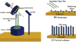
Double Schottky metal–semiconductor–metal based GaN photodetectors with improved response using laser MBE technique
Present work demonstrates the fabrication of Gallium nitride (GaN) based ultraviolet metal–semiconductor–metal (MSM) photodetectors on Si(111)...

-
Study of a Solar-Blind Photodetector Based on an IZTO/β-Ga2O3/ITO Schottky Diode
An InZnSnO 2 (IZTO)/β-Ga 2 O 3 solar blind Schottky barrier diode photodetector (PhD) exposed to 255 nm, 385 nm and 500 nm light wavelengths was...

-
Effect of titanium-dioxide nanoparticle on Richardson constant and barrier height of tartrazine dye based Schottky device
Recently Fruit Dyes have achieved a significant interest as organic devices because of they are widely available, customizable and biodegradable. But...

-
A study on electrical properties of Au/4H-SiC Schottky diode under illumination
In this work, a metal–semiconductor diode in the form of Au/4H-SiC is fabricated, and the electrical properties of this device are systematically...

-
On the wide range frequency and voltage dependence of electrical features and density of surface states of the Al/(Cu:DLC)/p-Si/Au Schottky diodes (SDs)
Due to their high dielectric strength, high resistivity, and extended range of band gap, diamond-like carbon films have great potential in the...

-
Investigation on the effect of metal contacts on the vertical MnO2 nanowire array-based Schottky barrier diodes
This work reflects the successful fabrication of manganese dioxide (MnO 2 ) nanowires (NW) by glancing angle deposition technique. The impact of metals...
-
Indium gallium nitride on silicon heterojunction Schottky barrier solar cell characteristics
We present calculations of performance characteristics of Indium Gallium Nitride-Silicon Heterojunction Schottky barrier solar cells. The effect of...

-
Barrier reduction and current transport mechanism in Pt/n-InP Schottky diodes using atomic layer deposited ZnO interlayer
Modification of interface properties in Pt/n-InP Schottky contacts with atomic layer deposited ZnO interlayer (IL) (5 and 10 nm) has been carried out...

-
The effect of thermal annealing on Ti/p-Si Schottky diodes
Ti/ p -Si Schottky barrier diodes (SBDs) have been prepared by metal evaporating method. The effect of low annealing temperature on electrical...

-
The current–voltage characteristics of V2O5/n-Si Schottky diodes formed with different metals
In this work, we reported the effect of different metal contacts on performance of metal–oxide–semiconductor (MOS)-structured Schottky diodes formed...

-
Rapidly and mildly transferring anatase phase of graphene-activated TiO2 to rutile with elevated Schottky barrier: Facilitating interfacial hot electron injection for Vis-NIR driven photocatalysis
Visible and even infrared (IR) light-initiated hot electrons of graphene (Gr) catalysts are a promising driven power for green, safe, and sustainable...

-
Effect of amorphous SiC layer on electrical and optical properties of Al/a-SiC/c-Si Schottky diode for optoelectronic applications
In this work, we report on the study of the electrical and optical properties of amorphous silicon carbide (a-SiC)-based Schottky diodes for...

-
A comparison electrical characteristics of the Au/(pure-PVA)/n-Si and Au/(CdTe doped-PVA)/n-Si (MPS) type Schottky structures using I–V and C–V measurements
In this study, both the Au/(pure-PVA)/n-Si (MPS-1) and Au/(CdTe:PVA)/n-Si (MPS-2) type Schottky diodes (SDs) were fabricated onto the same n-Si wafer...

-
Effect of an ITIC non-fullerene interlayer on electrical properties and external quantum efficiency of Al/ZnO/p-Si Schottky photodiodes
Metal-semiconductor (MS) heterojunctions are one of the main components of today’s technology. In the production of metal-semiconductor...

-
Vertical GaN Schottky Barrier Diode Using Nitrogen Ion Implantation to Form a Donut-Shaped Channel
This paper proposes the use of nitrogen ion implantation to form circular and donut-shaped channels in vertical GaN Schottky barrier diodes (SBDs)....

-
The investigation of current-transport mechanisms (CTMs) in the Al/(In2S3:PVA)/p-Si (MPS)-type Schottky barrier diodes (SBDs) at low and intermediate temperatures
The current-transport mechanisms (CTMs) and temperature sensitivities ( S ) of the Al/(In 2 S 3 -PVA)/p-Si SBDs have been investigated using I–V ...

-
Au–Ag binary alloys on n-GaAs substrates and effect of work functions on Schottky barrier height
In this study, I investigated the effect of work function ( ϕ m ) of Au x Ag 1− x ( x = 0, 0.22, 0.37, 0.71 and 1) on the Au–Ag/n-GaAs Schottky diode (SD)...

-
Dependence of Electrical Properties of Ni/n-GaP/Al Schottky Contacts on Measurement Temperature and Thermal Annealing
Ni/ n -GaP/Al Schottky diodes have been fabricated and thermally annealed at 400°C to obtain Schottky rectifying contacts with optimum performance and...

-
Characteristics of 21H-SiC Thin Film-Based Schottky Barrier Diodes Using TiN Contacts
The fabrication of Schottky barrier diodes based on thin films of 21H polytype of SiC is reported. The films were deposited using a single composite...