Search
Search Results
-
Reduced Threading Dislocation Density in a Ge Epitaxial Film on a Submicron-Patterned Si Substrate Grown by Chemical Vapor Deposition
A patterned Si substrate is used to reduce the threading dislocation density (TDD) in a Ge epitaxial film for near-infrared photonic device...

-
Investigating the edge effects of Cu electroplating on the SAMs-coated Si substrate
Self-assembled monolayers (SAMs) are used to pattern the surface for metal deposition to study its effect on Cu deposition. Here, Cu...

-
Design and tailoring of patterned ZnO nanostructures for perovskite light absorption modulation
Lithography is a pivotal micro/nanomanufacturing technique, facilitating performance enhancements in an extensive array of devices, encompassing...
-
Regulating Effect of Substrate Temperature on Sputtering-grown Ge/Si QDs under Low Ge Deposition
The effect of deposition temperature on the morphology and optoelectronic performance of Ge/Si QDs grown by magnetron sputtering under low Ge...
-
High-Pixel-Density Fine Metal Mask Fabricated by Electroforming of Fe-Ni Alloy onto UV-nanoimprinted Resin Pattern on Si Substrate
A fine metal mask (FMM) used for vacuum evaporation of electroluminescent material in organic light-emitting diode display is demonstrated using UV...

-
Templated synthesis of patterned gold nanoparticle assemblies for highly sensitive and reliable SERS substrates
Formation of plasmonic structure in closely packed assemblies of metallic nanoparticles (NPs) is essential for various applications in sensing,...

-
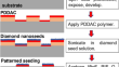
Effect of CH4 concentration on the early growth stage of patterned diamond using high seeding density and hot filament chemical vapor deposition
A bottom-up method is described to grow patterned polycrystalline diamond on silicon substrates using polymer assisted seeding and photolithography....
-
Strategies for dislocation density reduction in CdTe epilayers grown directly on (211) Si substrates using MOVPE
Two different techniques, namely in-situ cycle annealing and post-growth patterning and annealing, were studied to reduce dislocation density in...

-
Mechanical behavior of surface-patterned and coated Si or Ge wafers for superhydrophobic and antireflective light transmitting windows
The compressive resistance of truncated nanocone lattices produced by lithography and etching steps on Si or Ge wafers to get superhydrophobic and...

-
Dislocation Density Reduction in MOVPE-Grown (211) CdTe/Si by Post-Growth Patterning and Annealing
We studied the effectiveness of post-growth patterning and annealing on threading dislocation (TD) reduction in (211) CdTe/Si epilayers grown using...

-
Controlled epitaxy and patterned growth of one-dimensional crystals via surface treatment of two-dimensional templates
Mixed-dimensional van der Waals (vdW) heterostructures offer promising platforms for exploring interesting phenomena and functionalities. To exploit...

-
Infrared Absorption in Silicon Nanostructure-Patterned Absorber
Nanostructures or microstructure-patterned based metamaterials are fabricated on semiconductors’ surface to reduce the reflection and enhance the...
-
Van der Waals integration inch-scale 2D MoSe2 layers on Si for highly-sensitive broadband photodetection and imaging
As one of the most promising materials for two-dimensional transition metal chalcogenides (2D TMDs), molybdenum diselenide (MoSe 2 ) has great...

-
Inkjet printing of 2D polyaniline for fabricating flexible and patterned electrochromic devices
Conjugated organic polymer (COP)-based electrochromic devices (ECDs) exhibit promising applications in digital and color displays. However,...

-
Light trap** enhanced broadband photodetection and imaging based on MoSe2/pyramid Si vdW heterojunction
Two-dimensional (2D) layered materials have been considered promising candidates for next-generation optoelectronics. However, the performance of 2D...

-
Atomic layer annealing with radio-frequency substrate bias for control of grain morphology in gallium nitride thin films
AbstractA method of performing atomic layer annealing (ALA) with radio-frequency (RF) substrate bias on insulating and amorphous substrates is...

-
Magnetodynamic properties on square patterned of FeGaB and Al2O3/FeGaB thin films
This article shows low dam** patterned FeGaB and Al 2 O 3 /FeGaB thin films. FeGaB has a lower dam** factor (0.0071) than the Al 2 O 3 /FeGaB thin film....

-
A novel approach to Si0.5Ge0.5 channel FinFET fabrication: utilizing a three-layer SiGe strain relaxation buffer and In-Situ phosphorus do**
In this paper, a novel in-situ phosphorus doped three-layer SiGe strain relaxed buffer (SRB) is proposed in order to realize the integration of...

-
Selective Area Epitaxy of Complex Oxide Heterostructures on Si by Oxide Hard Mask Lift-Off
Epitaxial complex oxide heterostructures on Si are an excellent platform for the realization of multifunctional electronic devices to exploit the...

-
Single-material MoS2 thermoelectric junction enabled by substrate engineering
To realize a thermoelectric power generator, typically, a junction between two materials with different Seebeck coefficients needs to be fabricated....
