Search
Search Results
-
Ultrafast Scanning Tunneling Microscopy: Principles and Applications
The growing field of nanotechnology requires special tools capable of probing ultrafast surface dynamics on atomic scales in order to unveil...
-
Applications of Electrochemical Scanning Tunneling Microscopy in Corrosion Research
Scanning tunneling microscopy is a technique that is used to image atomic resolution conducting surfaces, find the density of states of the sample...
-
Recent progress in the role of grain boundaries in two-dimensional transition metal dichalcogenides studied using scanning tunneling microscopy/spectroscopy
Grain boundaries (GBs) are one- or two-dimensional (2D) defects, which are universal in crystals and play a crucial role in determining their...
-
Disentangling the electronic structure of an adsorbed graphene nanoring by scanning tunneling microscopy
Graphene nanorings are promising model structures to realize persistent ring currents and Aharonov–Bohm effect at the single molecular level. To...

-
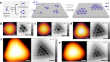
Ultrafast nanoscale exciton dynamics via laser-combined scanning tunneling microscopy in atomically thin materials
Long-term stable excitons, bound pairs of electrons and holes, in van der Waals materials were found to be handled at room temperature, paving the...

-
Investigation of charge transfer between donor and acceptor for small-molecule organic solar cells by scanning tunneling microscopy and ultrafast transient absorption spectroscopy
Small-molecule organic solar cell is a category of clean energy potential device since charge transfers between donor and acceptor. The morphologies,...

-
Scanning Electron Microscopy (SEM)
Scanning electron microscopy (SEM) is perhaps the first technique a catalyst researcher should use to start characterizing a catalyst. In this...
-
Scanning tunneling microscopy of buried dopants in silicon: images and their uncertainties
The ability to determine the locations of phosphorous dopants in silicon is crucial for the design, modelling, and analysis of atom-based nanoscale...

-
Machine learning for automated experimentation in scanning transmission electron microscopy
Machine learning (ML) has become critical for post-acquisition data analysis in (scanning) transmission electron microscopy, (S)TEM, imaging and...

-
Electrochemical scanning probe microscopies for artificial photosynthesis
The rational design of efficient artificial photosynthetic components requires thorough understandings towards (photo)electrochemical properties and...

-
Deep learning for electron and scanning probe microscopy: From materials design to atomic fabrication
Machine learning and artificial intelligence (ML/AI) are rapidly becoming an indispensable part of physics research, with applications ranging from...

-
Autonomous scanning probe microscopy investigations over WS2 and Au{111}
Individual atomic defects in 2D materials impact their macroscopic functionality. Correlating the interplay is challenging, however, intelligent...

-
Dynamic behavior of tunneling triboelectric charges in two-dimensional materials
Although the research history of triboelectrification has been more than 2000 years, there are still many problems to be solved so far. The use of...
-
Scanning Probe Microscopies (SPMs)
Part I: Atom Force Microscope (AFM) belongs to the family of scanning probe microscopes (SPMs) where a very sharp probe scans the surface in a full-...
-
Electron Microscopy
The chapter presents the fundaments of electron and optical microscopes. It begins with an overview of microscopy and then continues to how the...
-
Transmission, Scanning Transmission, and Scanning Electron Microscopy
The properties of magnetic materials are closely related to their microstructure and micromagnetic structures like magnetic domains and spin...
-
New Frontiers in Microscopy
This chapter deals with techniques that are not directly related to identification of minerals under microscope but for specialized investigation...
-
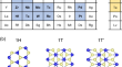
Chevron-type graphene nanoribbons with a reduced energy band gap: Solution synthesis, scanning tunneling microscopy and electrical characterization
Graphene nanoribbons (GNRs) attract a growing interest due to their tunable physical properties and promise for device applications. A variety of...

-
Atomic force microscopy with qPlus sensors
Atomic force microscopy is one of the most important tools in nanoscience. It employs an atomic probe that can resolve surfaces with atomic and...

-
Unidirectional alignment and orientation pinning mechanism of h-BN nucleation on Ir(111) via reactive probe atomic force microscopy
The epitaxial growth of wafer-scale single-crystalline two-dimensional materials requires precise control over the crystallographic orientation and...