Search
Search Results
-
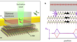
A visible-light-assisted Pd/TiO2 gas sensor with carbon nanotubes electrodes for trace formaldehyde detection
Owing to the ppb-level detection standard toward the toxic and harmful gas, the detection of trace gases has become an important subject in the field...

-
Single-crystalline nanoribbon network field effect transistors from arbitrary two-dimensional materials
The last decade has seen a flurry of studies related to graphene nanoribbons owing to their potential applications in the quantum realm. However,...

-
Low-k Dielectric for Semiconductor Packaging: Advancements, Challenges, and Future Outlook
This chapter examines the significance of low-k dielectric materials in semiconductor packaging. Low-k dielectrics play a critical role in reducing...
-
Wet sandblasting pretreatment of diamond wire sawn multi-crystalline silicon wafer for surface acid texturization in photovoltaics
As the substrate of photovoltaic solar cells, multi-crystalline silicon (mc-Si) wafers cut by diamond wire saw are less effective in commercial acid...

-
Technology/Nuts and Bolts
Basic microelectronics processing technology as well as some micromachining processes for silicon, used for fabricating the biosensors, are briefly...
-
Design and Fabrication of Wearable Biosensors: Materials, Methods, and Prospects
“Objects and their manufacture are inseparable. You understand a product if you understand how it’s made.” – Jonathan Ive.
-
Graphene-Based Interconnect for Semiconductor-Plausible Goal or Elusive Goal?
The continuous miniaturization and increasing complexity of semiconductor devices have necessitated the development of advanced interconnect...
-
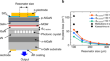
β-Ga2O3 Schottky Barrier Diodes with Near-Zero Turn-on Voltage and Breakdown Voltage over 3.6 kV
Lateral Schottky barrier diodes (SBD) were fabricated on a molecular beam epitaxy (MBE) grown, Si-doped β -Ga 2 O 3 wafer measuring 1 cm by 1.5 cm. These...

-
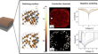
Emergence of layered nanoscale mesh networks through intrinsic molecular confinement self-assembly
Block copolymer self-assembly is a powerful tool for two-dimensional nanofabrication; however, the extension of this self-assembly concept to complex...

-
A soft, high-density neuroelectronic array
Techniques to study brain activities have evolved dramatically, yet tremendous challenges remain in acquiring high-throughput electrophysiological...

-
Nitrogen-vacancy magnetometry of CrSBr by diamond membrane transfer
Magnetic imaging using nitrogen-vacancy (NV) spins in diamonds is a powerful technique for acquiring quantitative information about sub-micron scale...
-
Wide-bandgap GaN-based watt-class photonic-crystal lasers
Short-wavelength (blue-violet-to-green) lasers with high power and high beam quality are required for various applications including the machining of...
-
High-resolution light-emitting devices for display applications
As carriers of visual information, displays play an indispensable role in our daily life. In recent years, high-resolution (HR) self-emissive...

-
Plasma Treatment for Surface Stabilization in InAs/GaSb Type-II Superlattice LWIR and VLWIR Photodetectors
An InAs/GaSb nBn structure was investigated as a replacement for mercury cadmium telluride (MCT) in long-wavelength infrared (LWIR) and very...

-
Recent progresses in thermal treatment of β-Ga2O3 single crystals and devices
In recent years, ultra-wide bandgap β-Ga 2 O 3 has emerged as a fascinating semiconductor material due to its great potential in power and photoelectric...
-
Nanosheet integration of induced tunnel field-effect transistor with lower cost and lower power
Nanosheet transistors are poised to become the preferred choice for the next generation of smaller-sized devices in the future. To address the future...

-
Functionalized nanowires for miRNA-mediated therapeutic programming of naïve T cells
Cellular programming of naïve T cells can improve the efficacy of adoptive T-cell therapy. However, the current ex vivo engineering of T cells...

-
Highly-efficient thin film LiNbO3 surface couplers connected by ridge-waveguide subwavelength gratings
The ridge waveguide integrated grating couplers (GCs) in lithium niobate on insulator (LiNbO 3 , LNOI) were designed, fabricated and characterized. Two...

-
Understanding the Electrical Characteristics of Electrochemical Metallization Memristors through Identification of Conduction Channel in Entire Active Area
Physical observation of electrochemical metallization (ECM) channel is required for understanding the electrical characteristics of ECM memristors....
-
Design and Analysis of Chalcogenide GeAsSe Waveguide for Dispersion Properties
This paper reports the design and analysis of a Ge11.5As24Se64.5 chalcogenide optical waveguide. The structure consists of Ge11.5As24Se64.5 as a core...