Search
Search Results
-
Metalorganic Chemical Vapor Deposition 1
This chapter is devoted to the growth of Ga2O3 and its alloys by metalorganic chemical vapor depositionMetalorganic chemical vapor deposition MOCVD...
-
Recent Development in the Preparation of Ferroelectric Thin Films by MOCVD
Recent research by our group, concerned with the preparation of ferroelectric thin films by MOCVD, is summarized. MOCVD has been investigated as a...
-
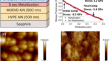
Demonstration of MOCVD-grown Ga2O3 power MOSFETs on sapphire with in-situ Si-doped by tetraethyl orthosilicate (TEOS)
In this work, we demonstrated Ga 2 O 3 -based power MOSFETs grown on c-plane sapphire substrates using in-situ TEOS do** for the first time. The β -Ga 2 O 3 ...

-
Unintentional do** effect in Si-doped MOCVD β-Ga2O3 films: Shallow donor states
High-quality β -Ga 2 O 3 films were epitaxially grown by using metalorganic chemical vapor deposition (MOCVD) with different donor concentrations, and...

-
Metal Organic Chemical Vapor Deposition 2
This chapter reviews the heteroepitaxial growthHeteroepitaxial growth of \(\upalpha \)- -GaO, - -GaO, and \(\upvarepsilon \)-gallium oxideGallium...
-
β-Ga2O3 MOSFETs electrical characteristic study of various etching depths grown on sapphire substrate by MOCVD
β-Ga 2 O 3 thin films with both a 45 nm Si-doped conductive epilayer and unintentionally doped epilayer were grown on c-plane sapphire substrate by...

-
Effects of Pre-Metallization on the MOCVD Growth and Properties of Ge-doped AlGaN on AlN/Sapphire Templates
The effects of pre-metallization of the growth surface on film stress and structural properties of undoped and Ge-doped Al x Ga 1−x N ( x ~ 0.5–0.6)...
-
Gas source chemical vapor deposition of hexagonal boron nitride on C-plane sapphire using B2H6 and NH3
Chemical vapor deposition (CVD) of hexagonal boron nitride (hBN) using diborane (B 2 H 6 ) and ammonia (NH 3 ) is reported. The effect of growth conditions...

-
Effect of metal source variation in cuprous oxide thin films deposited by chemical bath deposition
In this study, the effect of copper source in cuprous oxide thin films deposited by chemical bath deposition is presented. The replacement of copper...

-
Deposition of SrCO3 thin film consisting of self-assembled bundles of nanostructures by a plasma-enhanced liquid injection chemical vapour deposition technique
In this work, we demonstrate the deposition of SrCO 3 thin film consisting of SrCO 3 nano rods by a liquid injection plasma enhanced chemical vapour...

-
Mist Chemical Vapor Deposition 2
ε-Ga2O3Ε-Ga2O3 is one of the five polymorphs of Ga2O3, which has attracted considerable attention because it exhibits unique polarization and...
-
In- and out-plane transport properties of chemical vapor deposited TiO2 anatase films
AbstractDue to their polymorphism, TiO 2 films are quintessential components of state-of-the-art functional materials and devices for various...

-
Nonpolar AlxGa1−xN/AlyGa1−yN multiple quantum wells on GaN nanowire for UV emission
Nonpolar m -plane AlGaN offers the advantage of polarization-free multiple quantum wells (MQWs) for ultraviolet (UV) emission and can be achieved on...

-
Mist Chemical Vapor Deposition 1
This chapter summarizes fundamental issues of corundum-structured gallium oxide (α-Ga2O3)(-GaO , which is obtained by heteroepitaxy on sapphire...
-
Evaluation of MoS2 Films Fabricated by Metal-Organic Chemical Vapor Deposition Using a Novel Mo Precursor i-Pr2DADMo(CO)3 Under Various Deposition Conditions
Molybdenum disulfide (MoS 2 ) is expected to be applied for devices in various fields owing to its unique characteristics. Establishing a...
-
High-Gain and Low-Dark Current GaN p-i-n Ultraviolet Avalanche Photodiodes Grown by MOCVD Fabricated Using Ion-Implantation Isolation
Front-illuminated GaN-based p-i-n ultraviolet (UV) avalanche photodiodes (APDs) were grown by metalorganic chemical vapor deposition on a...

-
Pulsed laser deposition of nanostructured CeO2 antireflection coating for silicon solar cell
Increasing the power conversion efficiency (PCE) of silicon solar cells by improving their junction properties or minimizing light reflection losses...

-
High-quality GaN grown on nitrogen-doped monolayer graphene without an intermediate layer
GaN on graphene/Al 2 O 3 substrates grown via van der Waals epitaxy compensates for the deficiencies and defects caused by metal-organic chemical vapor...

-
Capacitor-on-Metal/Via-Stacked-Plug (CMVP) Memory Cell Technologies and Application to a Nonvolatile SRAM
A capacitor-on-metal/via-stacked-plug (CMVP) memory cell was developed for the 0.25 micr meter CMOS logic embedded FeRAM. Using a 445 C MOCVD...
-
Modeling of temperature-dependent photoluminescence of GaN epilayer by artificial neural network
Artificial neural networks (ANNs) are a type of machine learning model that are designed to mimic the structure and function of biological neurons....
