Search
Search Results
-
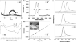
PbS colloidal quantum dots patterning technique with low vertical leakage current for the photodetection applications
The colloidal quantum dots (CQDs) are a promising nanometer-sized material system for optoelectronic applications due to the low cost, room...

-
Fully printed IGZO memristor arrays with robust threshold switching characteristics for artificial nociceptors
The large-scale fabrication and patterning of artificial perceptual systems are vital for the development of bionic systems. Traditional patterning...

-
Periodic surface functional group density on graphene via laser-induced substrate patterning at Si/SiO2 interface
Controlling the spatial distribution of functional groups on 2D materials on a micrometer scale and below represents a fascinating opportunity to...

-
Advances in lithographic techniques for precision nanostructure fabrication in biomedical applications
Nano-fabrication techniques have demonstrated their vital importance in technological innovation. However, low-throughput, high-cost and intrinsic...

-
Coat-and-print patterning of silver nanowires for flexible and transparent electronics
Silver nanowires (Ag NWs) possess excellent optoelectronic properties, which have led to many technology-focused applications of transparent and...

-
Direct laser patterning of two-dimensional lateral transition metal disulfide-oxide-disulfide heterostructures for ultrasensitive sensors
Two-dimensional (2D) heterostructures based on the combination of transition metal dichalcogenides (TMDs) and transition metal oxides (TMOs) have...

-
High-NA EUV: Prospects and Challenges and Stochastic Defects Related Manufacturing Yield Loss
High-NA EUV lithography deemed as the most successful patterning technique for feature sizes as low as 2–3 nm for FET architectures is reviewed for...
-
Strategies for dislocation density reduction in CdTe epilayers grown directly on (211) Si substrates using MOVPE
Two different techniques, namely in-situ cycle annealing and post-growth patterning and annealing, were studied to reduce dislocation density in...

-
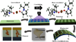
Patchy nanoparticles with surface complexity for directed self-assembly
Patchy nanoparticles (PNPs) possess anisotropic surfaces that produce emergent directionalities in interactions. Manipulation of such surface...

-
Tunable neuronal scaffold biomaterials through plasmonic photo-patterning of aerogels
The authors have shown recently that the neurite extension by neuronal PC12 cells is greatly impacted by aerogel topography. Indeed, the average...

-
Spatiotemporal control of liquid crystal structure and dynamics through activity patterning
Active materials are capable of converting free energy into mechanical work to produce autonomous motion, and exhibit striking collective dynamics...

-
Towards micro-PeLED displays
The miniaturization of conventional light-emitting diodes (LEDs) is a growing trend for emerging virtual and augmented reality and...

-
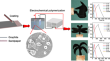
An agar sandwich method for patterning transparent conducting oxides
Transparent electrodes are frequently used to drive opto-electronic devices, and the patterning of these electrodes is essential. The present work...

-
Plasma-based processes for planar and 3D surface patterning of functional nanoparticles
We present a gas-phase process for surface patterning and 3D self-assembly of nanoparticles (NPs) of functional materials such as metals, oxides, and...

-
Cr-Photocrosslinked Polyvinylpyrrolidone Memristor: A Flexible, Rapid Manufacturing and Disposable Polymeric Electronic Memory Device
The fabrication of organic electronic memories requires the availability of patterning techniques. However, photolithography processes are not...
-
Cu(In,Ga)Se2 based ultrathin solar cells the pathway from lab rigid to large scale flexible technology
The incorporation of interface passivation structures in ultrathin Cu(In,Ga)Se 2 based solar cells is shown. The fabrication used an industry scalable...

-
Hydrophobic recovery of cross-linked polydimethylsiloxane films and its consequence in soft nano patterning
Cross-linked polydimethylsiloxane (PDMS) films and surfaces obtained by thermal cross-linking of commercially available Sylgard 184 are widely...

-
Structuring Surfaces at the Speed of Light
An emerging laser-based surface structuring technology (DLIP) uses the interference of light to transfer to materials well-defined periodic features...

-
A facile patterning preparation of barnacle-like polypyrrole on sandpaper for flexible electronics
The exploration of future energy storage devices with lightweight, flexible, and highly efficient energy management strategy has attracted increased...
-
Review of photoreduction and synchronous patterning of graphene oxide toward advanced applications
In view of the bulk production, resolvability, dispersibility of aqueous solution, graphene oxides (GO) prepared by strong chemical oxidation of...