Search
Search Results
-
Enhancement noise margin and delay time performance of novel punch-through nMOS for single-carrier CMOS
In this paper, we propose the use of punch-through nMOS (PTnMOS) as an alternative to pMOS in complementary metal oxide semiconductor (CMOS)...

-
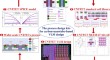
3D Stacked IC Chip Design: From CMOS to 2D Materials
The constant demand for higher performance and increased functionality in electronic devices has driven the evolution of integrated circuit (IC) chip...
-
CMOS compatible 2T pixel for on-wafer in-situ EUV detection
A novel 2-transistor (2T) pixel EUV detector is proposed and demonstrated by advanced CMOS technology. The proposed 2T detector also exhibits high...

-
Wafer-scale carbon-based CMOS PDK compatible with silicon-based VLSI design flow
Carbon nanotube field-effect transistors (CNTFETs) are increasingly recognized as a viable option for creating high-performance, low-power, and...
-
Wafer-scale fabrication of carbon-nanotube-based CMOS transistors and circuits with high thermal stability
Thanks to its single-atomic-layer structure, high carrier transport, and low power dissipation, carbon nanotube electronics is a leading candidate...

-
Embedded Micro-detectors for EUV Exposure Control in FinFET CMOS Technology
An on-wafer micro-detector for in situ EUV (wavelength of 13.5 nm) detection featuring FinFET CMOS compatibility, 1 T pixel and battery-less sensing...

-
Preparation and characterization of hafnium-zirconium oxide ceramics as a CMOS compatible material for non-volatile memories
Hf x Zr 1− x O 2 (HZO) ceramics with x = 0.25, 0.50 and 0.75 were prepared by conventional solid-state reaction technique. Structural studies of the...

-
Scalable CMOS back-end-of-line-compatible AlScN/two-dimensional channel ferroelectric field-effect transistors
Three-dimensional monolithic integration of memory devices with logic transistors is a frontier challenge in computer hardware. This integration is...

-
Limitation of CMOS Scaling and Effects of Parasitic Elements on the RF Performance
The invention of the transistor marked a pivotal moment in microelectronics, enabling the development of smaller, more efficient electronic devices....
-
Efficient charge carrier control on single walled carbon nanotube thin film transistors using water soluble polymer coatings
SWCNT-based thin-film transistors (TFTs) typically display unipolar p-type electrical characteristics in ambient condition due to the O 2 /H 2 O redox...

-
Ab initio perspective of ultra-scaled CMOS from 2D-material fundamentals to dynamically doped transistors
Using accurate dissipative DFT-NEGF atomistic-simulation techniques within the Wannier-Function formalism, we give a fresh look at the possibility of...

-
A Cu Pillar Bump Bonding Method Using Au-Sn Alloy Cap as the Interconnection Layer
High-temperature and flux-free bonding is important for heterogeneous integration of different chips. In this work, a Cu pillar bump was prepared by...

-
Recent progresses of NMOS and CMOS logic functions based on two-dimensional semiconductors
Metal-oxide-semiconductor field effect transistors (MOSFET) based on two-dimensional (2D) semiconductors have attracted extensive attention owing to...

-
Design of Hetero-Dielectric Single-Metal Gate-All-Around MOSFET with Schottky Contact Source/Drain
One of the most promising device configurations for extending CMOS device scaling is the gate-all-around MOSFET since it provides excellent...
-
Results: Integrating the Supersaturated Material in a CMOS Pixel Matrix
The information contained in this chapter is the result of the collaboration between the UCM and STMicroelectronics, through an internship financed...
-
The Application of FeRAM to Future Information Technology World
The future information technology world needs a simple identification and secure information storage medium. The advanced smart card is a...
-
How to build good inverters from nanomaterial-based transistors
As promising components of future integrated circuits (ICs), field-effect transistors (FETs) based on semiconducting nanomaterials are being...

-
Two-dimensional vertical p-n diodes with sub-2-nm channel lengths
Ultra-scaled p-n diodes are essential to the development of complementary metal oxide semiconductor (CMOS) integrated circuits. However, realizing...

-
Ultra-low power neuromorphic obstacle detection using a two-dimensional materials-based subthreshold transistor
Accurate, timely and selective detection of moving obstacles is crucial for reliable collision avoidance in autonomous robots. The area- and...

-
Design and Modeling of Gate Engineered Tunnel Field-Effect Transistor
With complementary metal-oxide semiconductors (CMOS) as the dominant invention, microelectronic production has witnessed a dramatic improvement in...