Search
Search Results
-
Multilevel artificial electronic synaptic device of direct grown robust MoS2 based memristor array for in-memory deep neural network
With an increasing demand for artificial intelligence, the emulation of the human brain in neuromorphic computing has led to an extraordinary result...

-
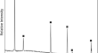
Kinetic mechanism of conformal magnesium silicide (Mg2Si) film formation via reaction of Si single crystals with Mg vapor
Patterned Mg 2 Si structures can be attractive for use in optoelectronic, thermoelectric, and other devices. Such structures can be fabricated as...
-
Effects of an interfacial layer on stress relaxation mechanisms active in the Cu-Si thin film system during thermal cycling
The authors report effects of placing a very thin metallic interlayer, such as W and Ni, in between the Cu film and the Si substrate on cyclic...

-
Fabrication and application of arrays related to two-dimensional materials
AbstractIn recent years, two-dimensional (2D) materials have attracted extensive attention from researchers for their unique structures and...
-
An integrated and robust plant pulse monitoring system based on biomimetic wearable sensor
Plant wearable sensors have potential to provide continuous measurements of plant physiological information. However, stable and high-fidelity...

-
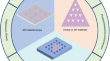
Inter-facet composition modulation of III-nitride nanowires over pyramid textured Si substrates by stationary molecular beam epitaxy
InGaN nanowires (NWs) are grown on pyramid textured Si substrates by stationary plasma-assisted molecular beam epitaxy (PA-MBE). The incidence angles...

-
Synthesis of Vertically Aligned ZnO Nanorods Using Sol-gel Seeding and Colloidal Lithography Patterning
Different ZnO nanostructures can be grown using low-cost chemical bath deposition. Although this technique is cost-efficient and flexible, the final...

-
A GQD-based composite film as photon down-converter in CNT/Si solar cells
Graphene quantum dots (GQDs), have unique quantum confinement effects, tunable bandgap and luminescence property, with a wide range of potential...

-
Bulk acoustic wave (BAW) resonator-based MEMS magnetic field sensor
This paper experimentally demonstrates a MEMS magnetic field sensor which is working at ∼ 0.873 GHz resonant frequency. The Bulk Acoustic Wave (BAW)...

-
Solving integral equations in free space with inverse-designed ultrathin optical metagratings
As standard microelectronic technology approaches fundamental limitations in speed and power consumption, novel computing strategies are strongly...

-
Photonic Curing of Copper Ink Films on Liquid Crystal Polymer Substrate
The application of intense pulsed light (IPL) to printed copper nanoparticle (CuNP) films enables rapid curing on low temperature substrates in...
-
Controlled nano structures on solution-processed inorganic/organic film for liquid crystal application
Ultraviolet (UV) nanoimprint lithography (NIL) was performed using a hybrid solution of ZnO and UV-curable polymer. The concentration of the...

-
Frequency Response Characteristics Depending on the Metal Cap** Structure and Length of the Amorphous SiZnSnO Thin Film Transistor
Amorphous oxide semiconductors (AOSs) have already been adopted as a channel layer in the display industry and have recently expanded their scope. A...

-
A soft, high-density neuroelectronic array
Techniques to study brain activities have evolved dramatically, yet tremendous challenges remain in acquiring high-throughput electrophysiological...

-
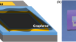
The effect of graphene layers on the optoelectronic properties of graphene–silicon photodetector
The graphene/silicon (g/Si) heterojunction has garnered significant attention due to the exceptional properties of graphene. As a result of...
-
Enhanced analog synaptic behavior of SiNx/a-Si bilayer memristors through Ge implantation
Conductive bridging random access memory (CBRAM) has been considered to be a promising emerging device for artificial synapses in neuromorphic...

-
On the Baliga’s Figure-Of-Merits (BFOM) Enhancement of a Novel GaN Nano-Pillar Vertical Field Effect Transistor (FET) with 2DEG Channel and Patterned Substrate
A novel enhancement-mode vertical GaN field effect transistor (FET) with 2DEG for reducing the on-state resistance ( R ON ) and substrate pattern (SP)...

-
Electrical Properties of Silicon Oxide Layers Subjected to High-Temperature Treatment Reproducing the Growth Conditions for Thin Carbon Films
The extraordinary behavior of the oxide charge in SiO 2 /Si structures processed under the conditions reproducing chemical-vapor-deposition (CVD)...

-
Understanding the Role of Near-Junction Diamond Heat Spreaders in Packaged 20-Gate GaN HEMT Chips via Thermal Simulation
The study of heat dissipation from GaN high-electron-mobility transistors (HEMT) is important for devising an effective thermal management strategy....

-
Chemiresistive Sensor Based on Redox-Active Porous Coordination Networks
By changing the rate of evaporation, two kinds of crystalline films composed of redox-active porous coordination networks (PCN 1 and 2) were...