Search
Search Results
-
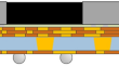
On the optimization of molding warpage for wafer-level glass interposer packaging
Through-glass-via (TGV) technology has great potential for various applications in advanced electronic packaging and integrated passive devices due...

-
Design Optimization of Pillar Bump Structure for Minimizing the Stress in Brittle Low K Dielectric Material Layer
Cu pillar bump offers a number of advantages for flip chip packaging, compared to the conventional solder bump. However, due to its rigidity...

-
Effect of pre-soldering temperatures on the microstructures and shear behaviors of SnBi-SAC/ENIG solder joints
Thermal deformation during soldering between the chip and the substrate is an important factor affecting the quality of high-density packaging of...

-
Development of high performance 2.5D packaging using glass interposer with through glass vias
2.5D interposer technology has gotten a lot of attention as a viable solution to high IO density, cost, and performance challenges. Glass is a...
-
Compact structured light generation based on meta-hologram PCSEL integration
Metasurfaces, a catalog of optical components, offer numerous novel functions on demand. They have been integrated with vertical cavity...

-
The In-Situ TEM Isothermal Aging Evolution in a µ-Cu/NiAu/Sn/Cu Solder Joint for Full Intermetallic Compounds Interconnects of Flexible Electronics
A structure composed of various Cu–Ni–Sn IMCs would develop from severe Joule heat and excessive elemental diffusion under high-density current in...

-
An Introduction of the Phosphor-Converted White LED Packaging and Its Reliability
Phosphor-converted white light-emitting diodes (pc-white LEDs) have attracted considerable attention as a new generation light source since the first...
-
Gold-coated tin oxide nanoparticles as potential optical isolator materials: simulation of absorption and Faraday rotation and comparison with micelle templated core-shell nanoparticles
On-chip optical isolation is currently one of the main challenges of photonic integrated circuits. Thus, there is a need for materials that exhibit...

-
A review on future novel interconnect and polymeric materials for cryogenic memory packaging
With the recent innovation of Open Artificial Intelligence, ChatGPT deployment as well as decarbonizing aviation such as future electric and hybrid...

-
Wafer-scale carbon-based CMOS PDK compatible with silicon-based VLSI design flow
Carbon nanotube field-effect transistors (CNTFETs) are increasingly recognized as a viable option for creating high-performance, low-power, and...
-
Failure behavior of flip chip solder joint under coupling condition of thermal cycling and electrical current
In this work, the failure behavior of a commercial chip size packaging (CSP) with flip chip solder joint was investigated under the coupling...

-
Die-embedded glass packaging for 6G wireless applications
This work presents the design and fabrication of an antenna-integrated glass package with embedded die for D-band (110–170 GHz) wireless...

-
Unraveling the spin current hermiticity
The effervescent area of spintronics has produced different fields of research; among them is the field of interface phenomena capable of revealing...

-
Low Temperature Flip Chip Bonding Using Squeegee-Embedded Au Nanoporous Bump Activated by VUV/O3 Treatment
This paper describes low-temperature bonding realized by squeegee-embedded Au nanoporous bumps that were activated by vacuum ultraviolet in the...
-
Flip-Chip Packaging for Nanoscale Silicon Logic Devices: Challenges and Opportunities
Semiconductor devices reached the nanoscale in the 2000s and have continued to shrink their features in accordance with Moore’s law. Semiconductor...
-

-
Comparison of the Microstructural Characteristics and the Electrothermal Fracture Mechanism of Au-Pd-Coated Copper Wire and Cu-Ti Micro-alloyed Wire
This study compared the Au-Pd-coated copper (CPA) with the micro-alloyed copper wires (MAC) without a coating layer. Results have shown that heat...

-
Nanowire ACF for Ultrafine-Pitch Flip-Chip Interconnection
Advanced microelectronic packaging, driven by the multiple benefits of system performance, power, size and cost, has moved into a three-dimensional...
-

-
Thermal and mechanical property of FCLED package component interconnected with Sn–MWCNT composite solder
Flip-chip light-emitting diode (FCLED) packages were interconnected with various contents of Sn-decorated multi-walled carbon nanotube (Sn–MWCNT)...
