Search
Search Results
-
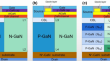
Projected performance of Si- and 2D-material-based SRAM circuits ranging from 16 nm to 1 nm technology nodes
Researchers have been develo** 2D materials (2DM) for electronics, which are widely considered a possible replacement for silicon in future...

-
Recent progresses in thermal treatment of β-Ga2O3 single crystals and devices
In recent years, ultra-wide bandgap β-Ga 2 O 3 has emerged as a fascinating semiconductor material due to its great potential in power and photoelectric...
-
Carbon materials: The burgeoning promise in electronics
Current electronic technology based on silicon is approaching its physical and scientific limits. Carbon-based devices have numerous advantages for...
-
Unintentional do** effect in Si-doped MOCVD β-Ga2O3 films: Shallow donor states
High-quality β -Ga 2 O 3 films were epitaxially grown by using metalorganic chemical vapor deposition (MOCVD) with different donor concentrations, and...

-
Characterization of Defect Structure in Epilayer Grown on On-Axis SiC by Synchrotron X-ray Topography
We observed the defect structure in the epilayer grown on an on-axis 4H-SiC substrate using synchrotron x-ray topography. The epilayer contained many...

-
Embedded Micro-detectors for EUV Exposure Control in FinFET CMOS Technology
An on-wafer micro-detector for in situ EUV (wavelength of 13.5 nm) detection featuring FinFET CMOS compatibility, 1 T pixel and battery-less sensing...

-
Field-Effect Transistors 5
Recently, significant progresses have been made on the demonstration and development of vertical gallium oxide power devices. The goal of this...
-
Evaluation of Anisotropic Biaxial Stress Induced Around Trench Gate of Si Power Transistor Using Water-Immersion Raman Spectroscopy
The trench gate structure is one of the promising techniques to reduce on-state resistance ( R on ) for silicon power devices, such as insulated gate...
-
Study of GaN-Based Superjunction CAVET with Dipole Layer to Further Improve On-Resistance and Breakdown Voltage
We propose a GaN-based superjunction current-aperture vertical electron transistor (CAVET) with a dipole layer (DL-SJ CAVET) and demonstrated...
-
Applicability of Channel Do** Gradient in the Design of a Short Channel (0.1 µm) LDMOS Transistor for Integrated Power and RF Applications
In this work, we have proposed a channel engineering technique for the performance enhancement of a short channel Laterally Diffused...

-
Investigation of the layout and optical proximity correction effects to control the trench etching process on 4H-SiC
Although trench gate and super-junction technology have micro-trench problems when applied to the SiC process due to the material characteristics. In...

-
Surface Functionalization of III–V Nanowires
The physical and chemical properties of semiconductor nanowires are significantly influenced by their surface structure and morphology. This can be...
-
Nanowire Field-Effect Transistors
Vertical field-effect transistors (FETs) using semiconductor nanowires (NWs) formed by bottom-up approach are expected to outperform conventional...
-
Carbon nanotube transistor technology for More-Moore scaling
Scaling of silicon field-effect transistors has fueled the exponential development of microelectronics in the past 60 years, but is now close to its...

-
Minimizing the TID effects due to gamma rays by using diamond layout for MOSFETs
This manuscript describes an experimental comparative study of effects of the total ionizing dose (TID) on the main electrical parameters and figures...

-
Device processing and junction formation needs for ultra-high power Ga2O3 electronics
A review is given of the future device processing needs for Ga 2 0 3 power electronics. The two main devices employed in power converters and wireless...

-
An insulated gate bipolar transistor with three-layer poly gate for improved figure of merit
In this study, an insulated gate bipolar transistor (IGBT) with three-layer poly gate is proposed and investigated by TCAD simulation. Here, gate is...

-
Ultrawide-bandgap (6.14 eV) (AlGa)2O3/Ga2O3 heterostructure designed by lattice matching strategy for highly sensitive vacuum ultraviolet photodetection
One judiciously designed strategy of utilizing an ultrathin but conductive Ga 2 O 3 :Si nanolayer to prepare (AlGa) 2 O 3 crystalline film is demonstrated....

-
Optoelectronic CMOS Transistors: Performance Advantages for Sub-7nm ULSI, RF ASIC, Memories, and Power MOSFETs
Substantial increase of output current, and I on / I off ratio for sub-7nm low power CMOS transistors, can be accomplished using a novel optoelectronic...
-
Uniformity of Gate Dielectric for I/O and Core HK/MG pMOSFETs with Nitridation Treatments
Uniformity consideration in integrated-circuit manufacturing is an impressive task, especially in the field of nano-node semiconductors. The use of...