
Abstract
The discovery of magnetic order in atomically-thin van der Waals materials has strengthened the alliance between spintronics and two-dimensional materials. An important use of magnetic two-dimensional materials in spintronic devices, which has not yet been demonstrated, would be for coherent spin injection via the spin-pum** effect. Here, we report spin pum** from Cr2Ge2Te6 into Pt or W and detection of the spin current by inverse spin Hall effect. The magnetization dynamics of the hybrid Cr2Ge2Te6/Pt system are measured, and a magnetic dam** constant of ~ 4–10 × 10−4 is obtained for thick Cr2Ge2Te6 flakes, a record low for ferromagnetic van der Waals materials. Moreover, a high interface spin transmission efficiency (a spin mixing conductance of 2.4 × 10¹⁹/m2) is directly extracted, which is instrumental in delivering spin-related quantities such as spin angular momentum and spin-orbit torque across an interface of the van der Waals system. The low magnetic dam** that promotes efficient spin current generation together with high interfacial spin transmission efficiency suggests promising applications for integrating Cr2Ge2Te6 into low-temperature two-dimensional spintronic devices as the source of coherent spin or magnon current.
Introduction
Magnetic two-dimensional (2D) van der Waals (vdW) systems have recently become a vibrant research field because of their exotic properties and central role in building 2D spintronic devices1,2,3,4,5. The spin injection is one of the most important aspects of spintronics, which lays the foundation for studying spin transport and relaxation in the low-dimensional systems in relation to other quantities like charge, valleys, lattice or band topology6,7,8,9. Making use of the magnetic 2D materials, people have realized spin injection into the nonmagnetic vdW materials through spin-polarized electron tunnelling10,11 and thermally-driven spin injection10,12. Beyond these methods, spin pum** driven by ferromagnetic resonance (FMR) is another well-established scheme13, and it has been widely used for spin injection from conventional magnetic materials into a great number of different systems: metals14, semiconductors15, topological insulators16,17, superconductors18 and quantum materials20,21. Therefore, considering the vast number of 2D materials, spin pum** based on vdW magnetic materials could significantly advance their applications in spintronic devices. This will not only benefit studies of the various spin-related phenomena in nonmagnetic vdW materials but also, in turn, the spin dynamic properties of the magnetic vdW systems. However, the use of magnetic vdW materials for coherent spin-pum** and its electrical detection has not yet been demonstrated. Two factors might hamper the development of this technique: suitable vdW magnets with relatively low magnetic dam** and high-quality interfaces for efficient transfer of spin angular momentum to adjacent materials. Closely related questions are whether the spin dynamic behaviour of the vdW magnet at the 2D limit (with strong spin fluctuations) deviates from that of an ultra-thin conventional magnet and how efficient the spin current transfer can be across the vdW gaps.
Here, we report efficient spin pum** from a layered ferromagnetic insulator, Cr2Ge2Te6 (CGT), into a heavy metal (HM), as shown in Fig. 1a. A state-of-the-art low magnetic dam** constant was obtained in the CGT/Pt bilayer from the frequency-dependent linewidth of the spin-pum** signals. This property suggests the CGT crystal can be a promising host material for transporting spin or magnon current (which can be excited incoherently or coherently) over long distances. The interface properties of CGT/Pt were directly investigated from the dependence of magnetic dam** on CGT thickness, and the spin mixing conductance was deduced. The magnetic dam** constants and interface spin mixing conductance of the CGT-based system at low temperatures are comparable to those of the benchmark yttrium iron garnet (YIG) spin-pum** system with ultra-low magnetic dam** at room temperature22. Moreover, in contrast to the fact that the spin-pum** efficiency of the YIG thin film-based system usually worsens when cooling below room temperature, the spin-pum** efficiency in CGT/Pt exhibits only a mild temperature dependence below 50 K. The CGT-based system is more appealing for coherent temperature-independent spin pum**. Our work reveals that CGT can efficiently generate dynamic spin currents and deliver them across the interface, which makes CGT an ideal 2D platform for studying spin dynamics in a low-dimensional hybrid system at low temperatures. For instance, using CGT as a coherent spin source and integrating it with a nonmagnetic transition metal dichalcogenide (TMD), one might seamlessly study the interplay between spin and other degrees of freedom including the valleys, symmetry, and twist angle of the heterostructures23,24. Although the working temperature of these heterostructures is currently limited by the relatively low Curie temperature of pristine CGT, our work highlights the potential of using CGT and other 2D magnets (including ferromagnets and antiferromagnets) as the coherent spin/magnon source in full-vdW spintronic devices and exploring emerging phenomena and device functions at the designed atomic interfaces and hybrid structures etc. Further understanding of the underlying mechanisms for low magnetic dam** in CGT and looking deep into the spin relaxation process across the interface helps to resolve the challenges of develo** more compact and versatile spintronics devices based on vdW materials in the future.

a Schematic illustration of the spin-pum** experimental set-up, where Hrf and Js stand for the oscillating magnetic field and d.c. spin current, respectively. b Atomic structure of CGT from top and side views, where a central Cr atom (magenta sphere) bonded to six ligand atoms (Te) consisting of a honeycomb network of edge-shared CrTe6 octahedra elongated by Ge dimers. c Raman spectra for various CGT/Pt thin films, which are detected from the spots shown in the inset (the red, magenta, blue and black colors correspond to the stacks with monolayer, bilayer, four-layer, and bulk CGT, respectively). d High-angle annular dark-field STEM image of the cross-section of a CGT/Pt bilayer, its interface region is marked by a white dashed rectangle with Au particles beneath the CGT. e The spin-pum** device layout, where the RF signal is introduced via the left side of Ground-Source-Ground (GSG) pads (which are isolated from CGT/HM stacks by a SiO2 layer), an oscillating RF magnetic field was generated perpendicular to the CGT stack. f Typical Hall resistance of a CGT/Pt bilayer, where the vanishing anomalous Hall resistance between 60 K and 70 K signifies a Curie temperature of around ~65 K. The scale bars are 200 µm, 5 nm, and 200 µm in (c), (d), and (e), respectively.
Results
Sample characterization and device fabrication
As one of the first-reported intrinsic 2D ferromagnets (FM), CGT has attracted tremendous attention1,25,26,27,28. Below Tc (~67 K for bulk material), the neighboring Cr atoms are ferromagnetically coupled to each other through Cr-Te-Cr bonds with a bond angle of ~90o (Fig. 1b). Being a nearly ideal 2D Heisenberg system, the magnetocrystalline anisotropy energy required for long-range ferromagnetic order is generated by a covalent bond between ligand Te-p and Cr-eg orbitals29. The magnetic properties of the bulk CGT used in this work are similar to those reported in the literature (Supplementary Fig. S1)30.
Thanks to the Au-assisted exfoliation method31, we managed to exfoliate bulk CGT into sub-millimeter size flakes of various thicknesses (inset of Fig. 1c and Methods). The final step of the exfoliation process was carried out in a high-vacuum chamber to avoid oxidizing the CGT surface32. The HM (Pt or W) thin films were subsequently grown onto the fresh surface of CGT by low-power sputtering (see Methods). The HM layer serves as the spin current detector via the inverse spin Hall effect (ISHE). Although we tried avoid it, some damage to the CGT surface during HM deposition was inevitable. For a single CGT monolayer covered by Pt (marked by a red dot and corresponding to the red curve in Fig. 1c), no characteristic 2D Raman spectrum is detectable, but for relatively thicker CGT flakes (two or more layers), the characteristic Eg2 and Ag2 Raman modes show up without any sign of oxidation (Methods)33. Figure 1d shows the cross-section of the CGT/Pt stack, acquired by aberration-corrected scanning transmission electron microscopy (STEM). Only the CGT/Pt interface layer is imperfect (see the white dashed rectangle region in Fig. 1d). The layered CGT beneath stays intact, consistent with the Raman spectra.
Figure 1e shows the device fabricated for the spin pum** measurement (see the other device geometry in Supplementary Fig. S6a). CGT/HM bilayers with a typical length of 300 µm were used (see the two CGT/HM stacks in Fig. 1e), which are capable of observing spin-pum** voltages (Vsp) with a high signal-noise ratio. The Hall bar devices were fabricated at the same time as the spin-pum** devices on the sub-mm flakes. The magnetic properties of the insulating CGT flakes are first probed by the anomalous Hall effect (AHE) in the CGT/Pt and CGT/W Hall-bar devices, as shown for Pt in Fig. 1f. For the CGT(12)/Pt(4), clear AHE signals are found below 70 K, which indicates that the Tc of 12 nm CGT is ~ 65 K (numbers in brackets throughout this paper are in nanometers). The Tc is consistent with the magnetic properties of bulk CGT with out-of-plane uniaxial magnetic anisotropy and also agrees with the previous reports of CGT/Pt34,35. Similarly, clear AHE signals are also observed in CGT/W bilayers (Supplementary Fig. S4). The observation of AHE proves the transfer of spin current through the CGT/HM interface, which prompts us to perform spin-pum** measurements in CGT/HM devices.
Electrical detection of spin-pum** in CGT/Pt and CGT/W
Figure 2a shows typical results for Vsp as the function of the external magnetic field for CGT/Pt at 30 K. It is noted that the probing direction, spin current, and magnetization orientation are mutually orthogonal in order to maximize the spin-pum** voltages (while their directions are different in the second device geometry, see Supplementary Fig. S6). In this case, Vsp can be calculated as36,37.
Here, e is the electron charge, \({\theta }_{{SH}}\) is the spin Hall angle, \({l}_{{sf}}\) is the spin diffusion length, L is the probe length, R is the resistance of the HM, f is the microwave frequency, P is the ellipticity correction factor, and \({g}_{{eff}}^{\uparrow \downarrow }\) is the effective interface spin mixing conductance. \(\Theta\) presents the precession cone angle, \(\Theta={h}_{{rf}}/\triangle H\ll 1\), where \({h}_{{rf}}\) and \(\triangle H\) are the microwave magnetic field and FMR linewidth. Note that linewidth scales linearly with the effective magnetic dam** (see below Eq. 2). It is clear from this formula that under fixed RF power and parameters of spin detector, the Vsp (spin-pum** efficiency) is proportional to the effective spin mixing conductance and is approximately inversely proportional to the square of the magnetic dam**.

a Typical signals from the CGT(23)/Pt(4) stack at 30 K under RF signal frequencies of 8 GHz and 12 GHz, the spin-pum** voltages (Vsp) with linewidth (ΔH) and resonance field (Hr) are extracted by fitting a Lorentzian function with a linear background. b Spin-pum** voltages from CGT(19)/W(4) stack where the Vsp is inverted as compared with CGT/Pt. c A series of Vsp from CGT/Pt device under a wide range of RF signal frequencies (8 − 40 GHz). d The resonance field as the function of RF frequency is nicely fitted with Kittel’s equation for CGT/Pt and CGT/W individually at 30 K.
Characteristic Lorentzian peaks emerge when scanning the in-plane magnetic field H for different microwave frequencies. The resonance peaks can be nicely fitted by a Lorentzian function with symmetric and antisymmetric components. The symmetric component originates from the spin-pum** effect14,36. The antisymmetric component, which usually originates from the spin rectification effect38, is more than an order of magnitude smaller because of the insulating property of CGT and the low level of anisotropic magnetoresistance in CGT/Pt (Supplementary Fig. S4c, d). Therefore, the spin rectification effect can be safely ignored in our devices, which is an advantage of using an insulating FM rather than a conducting FM to obtain cleaner spin-pum** signals. The off-resonance background signal probably results from the spin Seebeck effect due to heating of the system by microwave irradiation. A pair of peaks with opposite signs of Vsp are observed for different field directions, which is the direct evidence of spin pum**39. The two resonance peaks have almost the same height (differences are less than 5%), which excludes the field-independence heating effect reported in spin-pum** measurements15,40. The sign of Vsp for CGT/W stacks is always opposite to that CGT/Pt, (Fig. 2b) under the same experimental condition. This is inferred directly from Eq. 1 because of the opposite spin Hall angles of Pt and W, which is further evidence that pure spin currents are pumped out from the CGT and injected into the adjacent Pt and W layers39. The peaks are wider for CGT(19)/W(4) than for CGT(23)/Pt(4), which is mainly due to the larger spin Hall angle in W and perhaps different interface properties.
Figure 2c shows representative examples of Vsp at different microwave frequencies. It is noted that a broadband (2-40 GHz) radio frequency (RF) signal can be efficiently introduced into the CGT stacks in our set-up, and Vsp is linearly proportional to the RF power when it is not too high (10-20 dBm). The different peak heights are mainly due to the frequency-dependent microwave losses and ellipticity correction factors. Plotting frequency as a function of the resonant field Hr acquired from Lorentzian fitting (Fig. 2d), one can extract the effective demagnetization field, \(4\pi\)Meff, of the CGT and the gyromagnetic ratio γ by the fitting of the Kittel equation:
\(f=({{{{{\rm{\gamma }}}}}}/2\pi )\sqrt{{H}_{{{{{{\rm{r}}}}}}}({H}_{{{{{{\rm{r}}}}}}}+4\pi {M}_{{{{{{\rm{eff}}}}}}})}\) with \({{{{{\rm{\gamma }}}}}}={{{{{\rm{g}}}}}}{\mu }_{B}/\hslash\), \(4\pi {M}_{{{{{{\rm{eff}}}}}}}=4\pi {M}_{s}-2{K}_{{{{{{\rm{u}}}}}}}/{M}_{s}\). Ms and Ku stand for saturation magnetization and out-of-plane uniaxial magnetocrystalline anisotropy constant, respectively41. A negative Meff and a positive intercept on the Hr axis in the f-Hr plot indicate the perpendicular magnetic anisotropy (PMA) of the CGT crystals. The larger value of 4πMeff ~ −1560 G for CGT(23)/Pt(4) than that of CGT(19)/W(4) (~ −1110 G) might originate from their different interface properties. Note that for the devices with thicker CGT, multi-peak resonance was often observed (see Supplementary Note 5) which was thus fitted by the multi-Lorentzian function. It might be related to the multi-domain modes, standing spin-wave modes, or inhomogeneity of devices, etc40,42,43.
Temperature and thickness dependence of spin pum**
Figure 3a shows the temperature dependence of the resonance peaks for CGT(30)/Pt(4). Clear spin-pum** signals emerge when the temperature is lower than Tc. In fact, the resonance is still detectable when the temperature is slightly above the Tc (see the example of Vsp at 70 K in Supplementary Fig. S8). As the temperature decreases from slightly above Tc to well below it, Vsp changes non-monotonically, as shown in Fig. 3b for the main peak. When the temperature falls below 60 K, Vsp increases evidently, and its magnitude usually peaks at ~ 30 K and then slightly decreases with further decrease in temperature. The increasing spin-pum** signals with lowing temperature is mainly related to the development of magnetization. The decrease of Vsp in the lowest temperature regime is because of larger magnetic dam** (in other words ΔH, see Fig. 3c), which is expected from Eq. 1. This temperature dependence of Vsp (and the linewidth) was also observed at other frequencies (see the data in Supplementary Fig. S9) with a similar trend, which is distinct from abruptly quench of Vsp with decreasing temperature in the YIG/Pt bilayer system, as we discuss later.

a Temperature dependence of Vsp from CGT(30)/Pt(4) under 12 GHz RF excitation, where the results are fitted by three symmetric Lorentzian peaks (an example is shown for Vsp at 30 K). b The extracted Vsp of the main peak observed at 12 GHz and 28 GHz (see data on Supplementary Fig. S9) show a similar trend of temperature dependence. c Temperature dependence of linewidth of Vsp of the main peak at 12 GHz and 28 GHz. d f-H plots for CGT/Pt stacks with the thickest and thinnest CGT in this work. Kittel’s equation was used to fit the data points (extending to intercept with x-axis). The resulting g-factor and effective Ms of CGT are shown in (e) and (f) for CGT with different thicknesses at different temperatures. Note that the dashed black line in (e) marks the g-factor of free electron, and data for CGT(19)/W(4) are plotted as cyan curves in (e) and (f), and the solid lines in (b), (c), (e) and (f) are to guide the eye. Error bars throughout this paper correspond to standard errors.
By fitting Vsp at different temperatures for various thicknesses of CGT, we can calculate the values of \(\gamma\), Meff, and Ku for thin CGT flakes, which would be difficult to access from conventional FMR spectra because of the small volumes. Figure 3d shows the f-Hr plot for CGT/Pt stacks with the thickest and thinnest CGT flakes measured in this work. The smaller intercepts on the Hr-axis of the plot imply a lower Ku and PMA in the thinner CGT flakes. The different slopes of the asymptotes of the f-Hr plots at the large resonant fields reflect the change of gyromagnetic ratio and hence g-factor with temperature, as shown in Fig. 3e, which characterizes the contribution of orbital angular momentum to the magnetization. It is found in CGT(60)/Pt(4) that g = 2 at ~50 K, and it keeps increasing as the temperature decreases from 60 K (Fig. 3e). The same trend of temperature-dependent g-factor was reported in bulk CGT observed by conventional FMR42, which confirms the fidelity of our measurement. The deviation from g = 2 implies the presence of orbital angular momentum in bulk CGT. It may be due to a nonspherical charge distribution in the d shells preventing the complete quench of the orbital moment or it may be rooted in the spin-orbit interaction of CGT42,44. A similar trend appears for the thinner CGT devices with relatively larger decreases of g-factor when the temperature is close to Tc. Because the Tc of a 12 nm CGT flake is almost the same as that of bulk CGT (as shown in Fig. 1f), and the exact Ms of the CGT flakes are not detectable at this stage, it is reasonable to use the value of bulk CGT and the extracted Meff (Fig. 3f) to calculate the anisotropy energy of these various CGT flakes. Ku is in the range (1.5–3.9) × 105 erg/cm3 from 60 K to 10 K, which agrees with the values of bulk CGT (see Ref. 42. and Supplementary Fig. S1b). The larger PMA (larger magnitude of Meff) in thicker CGT at lower temperatures implies the bulk origin of PMA in CGT. However, the difference between CGT(23)/Pt(4) and CGT(19)/W(4) (with Ku ~ 3.1 × 10⁵ and 2.7 × 10⁵ erg/cm3 respectively at 10 K) indicates a contribution of the interfaces to the PMA.
Magnetic dam** constant and spin mixing conductance of CGT/Pt stacks
One can expect an enhancement of the Gilbert dam** in the spin-pum** measurement because additional magnetization dam** takes place via “pum**” of the excess angular momentum across the interface into the nonmagnet. On account of the small change of linewidth with scanning frequency, usually the broadband RF signal (10-40 GHz) is required to extract the effective magnetic dam**, αeff:
Here, \(\triangle {H}_{0}\) is inhomogeneous linewidth. From linear fitting of the frequency-dependent linewidth, \(\triangle H\), \({\alpha }_{{eff}}\) is calculated for these stacks with different thicknesses of CGT at different temperatures. Figure 4a shows the spin-pum** signals at different frequencies for the samples with different CGT thicknesses. The ΔH was obtained by Lorentzian fitting of Vsp to extract αeff based on Eq. 2 (Fig. 4b, d). An effective magnetic dam** constant as low as ~ 1 × 10⁻³ is deduced for the 60 nm-thick CGT at 50 K (see the raw data in Supplementary Fig. S10 and an even lower value ~ (4 ± 1) × 10−4 in the sample prepared by the improved sputtering recipe in Supplementary Fig. S6). These values are comparable to that of high-quality YIG thin films at room temperature45,46. YIG is a low-dam** magnetic insulator. The low magnetic dam** in CGT is the parameter that enables the observation of Vsp with high efficiency. Note a relatively large value of ΔH0 (30–60 Oe) was found for the CGT/Pt stacks (Fig. 4b), which implies a source of extrinsic dam** that may originate from the inhomogeneous effect. For thinner CGT-based devices, assuming the inhomogeneity-induced dam** is similar to that of the 60 nm-thick flake, the obvious enhancement of the effective dam** (Fig. 4b for the data at 30 K and Supplementary Fig. S11 for that at other temperatures) can only be ascribed to the spin-pum** effect. The effective magnetic dam** increases with the decreasing of CGT as predicted by the spin-pum** mechanism47:
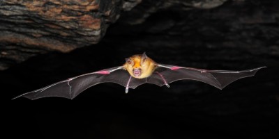
Here, \(t\) is the thickness of CGT, \({\mu }_{B}\) is the Bohr magneton, \({\alpha }_{{eff}}^{\infty }\) is the effective magnetic dam** of bulk CGT (with t → ∞) and \({\alpha }_{{SP}}\) accounts for the spin-pum** effect. Linearly fitting \({\alpha }_{{eff}}\) versus 1/t, we can extract the effective spin mixing conductance, \({g}_{{eff}}^{\uparrow \downarrow }\), for CGT/Pt interface (Fig. 4c). A deviation from linear behavior is found for t thinner than 14 nm. The magnetic properties of these thin CGT devices might be severely affected by inhomogeneous strain or the imperfect interfaces. From the fitting of data in the linear zone, a value of \({g}_{{eff}}^{\uparrow \downarrow }\) ~ 2.4 × 10¹⁹/m2 is obtained at 10 K. This value is comparable to that of YIG/Pt at room temperature48,49, which reflects its high efficiency of spin angular momentum transmission. Moreover, we find that \({g}_{{eff}}^{\uparrow \downarrow }\) decreases on rising temperature (~ 7 × 10¹⁸/m2 at 50 K, see Fig. 4f). It is distinct from the observation that for various FM/Pt bilayers (the FM can be a metal, a semiconductor, or YIG.) \({g}_{{eff}}^{\uparrow \downarrow }\) does not normally display obvious temperature dependence up to room temperature37.

a Vsp of CGT/Pt devices with different thicknesses of CGT under a range of RF frequencies to show the frequency and thickness dependence of the linewidth ΔH. From the left column to the right column, the frequencies are 11 GHz, 21 GHz, 31 GHz, and 40 GHz, respectively. b Linewidth vs frequency plotted for different thicknesses of CGT at 30 K, and linear fitting is used to derive the Gilbert dam**. c Change of effective Gilbert dam** with the thickness of CGT is displayed for extracting the contribution of spin pum** in the enhancement of magnetic dam** (only the linear regime was used. CGT/Pt devices with tCGT thinner than 14 nm and CGT/W are outside the linear zone). d ΔH-f plot for CGT(30)/Pt(4) at different temperatures. e Change of effective Gilbert dam** with temperature for CGT/Pt with different thicknesses of CGT. f Temperature dependence of spin-mixing conductance calculated from the linear fits in (c). The solid lines in (e) and (f) are to guide the eye.
As shown before, the linewidth of the spin-pum** signal also depends on the temperature. For the CGT(30)/Pt(4) sample, αeff decreases from 3.7 × 10⁻³ to 2 × 10⁻³ as the temperature increases from 10 to 50 K (Fig. 4e). While αeff in CGT(60)/Pt(4) remains almost unchanged below 40 K (although its anisotropy energy Ku almost doubles at 10 K), it slightly decreases at 50 K. Because of its large thickness, the spin-pum** contribution to αeff is not significant in CGT(60)/Pt(4). We speculate that the effective Gilbert dam** in bulk CGT is not sensitive to temperatures below 40 K. The obvious increase of αeff with decreasing temperature for thinner CGT is mainly due to the larger spin-pum** effect.
Discussion
One of the advantages of spin-pum** is the generation of coherent spin currents. As key evidence of coherent spin pum**, Vsp would ideally show no temperature dependence and only depend on the excitation power and rate of magnon relaxation39,40. However, coherent spin pum** generated by resonant excitation of magnons (with momentum k = 0 for FMR) could be accompanied by the incoherent spin-pum**, i.e., resonant heating causing a temperature gradient and pum** of spin current by the longitudinal spin Seebeck effect (LSSE). In the latter case, the incoherent thermal spin current falls with temperature and vanishes at T = 0 K50. Therefore, one might qualitatively estimate these two contributions to Vsp from its temperature dependence. For YIG/Pt, it was reported that the spin-pum** signal rapidly decreased on lowering the temperature below 200 K (see ref. 40,51,52, and Supplementary Fig. S9 for the case of YIG(50)/Pt(4) in our control sample). It was questioned whether coherent spin pum** is the main contribution to the observed large spin-pum** signals in the YIG/Pt system at room temperature40, although the severe decrease of the spin-pum** signal was also explained as an increase of Gilbert dam** in YIG due to impurity relaxation45,52. On the contrary, the Vsp signals in our CGT/Pt system only change slightly (for temperature ≤ 30 K, see Fig. 3b and Supplementary Fig. S9), and we will show that it can be explained by temperature-dependent interfaces properties. It suggests that the CGT offers much larger coherent spin-pum** signals at low temperatures than the thin-film YIG-based system.
Gilbert dam** is the intrinsic property of ferromagnetic materials that characterizes the rate of angular momentum dissipation into the lattice. It is the key parameter that determines the critical charge current density in magnetization switching and domain wall propagation speed, as well as spin-wave relaxation53,54,55. In principle, the Gilbert dam** of CGT can be measured by the FMR spectra of bulk CGT crystals56. However, because of the nonuniformity in the large crystals, their FMR spectra show much larger linewidths (Supplementary Note 2). Here, with the spin-pum** measurement on CGT/Pt devices, a relatively low magnetic dam** down to 4-10 × 10−4 was found for ferromagnetic insulator CGT (in the presence of spin-pum**), which is the lowest value yet reported in vdW magnetic systems (Table 1 and Supplementary Note 2). It is argued that this value is the upper limit of the intrinsic Gilbert dam** in CGT. In addition to the spin-pum** effect, the strain (exerted by the discontinuous Au nanoparticles during exfoliation) and the imperfect interface with the HM thin film can enhance the measured magnetic dam** in the form of inhomogeneous magnetization and two-magnon scattering55. However, the linear dependence of linewidth on frequency up to 40 GHz in all these devices indicates the minor contribution of two-magnon scattering54,57,58 (Supplementary Note 6). Nevertheless, the relatively low Gilbert dam** of the CGT flakes, comparable to that of high-quality epitaxial YIG thin films guarantees the potential application of CGT in spintronics, especially when combined with other vdW materials, e.g., TMDs and layered topological insulators, for studying the spin-charge interconversion. The low Gilbert dam** in CGT might be understood in two ways: the spin relaxation through spin-electron scattering is absent because it is insulating at low temperature; the weak spin-orbit interaction indicated by the tiny orbital magnetization (g ≈ 2) avoids the strong spin-phonon scattering44,59. Compared with the magnetic dam** of α ~ 6 × 10⁻³ for a 10.5 nm CGT flake extracted at frequencies of 2–22 GHz in a previous experiment by time-resolved Faraday rotation59, we have observed a considerably lower magnetic dam** constant in the relatively thicker CGT flakes. The discrepancy is probably related to the (thickness-dependent) crystal quality, and perhaps, more importantly, a wider frequency range (10–40 GHz) is required to extract the dam** constant.
The spin mixing conductance was also successfully extracted in our work for a hybrid interface with CGT. The values of \({g}_{{eff}}^{\uparrow \downarrow }\) at low temperature are even comparable to the values reported in metallic stacks37,60. On one hand, it reminds us that the interface between a vdW ferromagnet and normal metal is not an obstacle for spin transport as the spin angular moments were efficiently delivered across the interfaces in our spin-pum** experiment. It is thus consistent with the reports of highly-efficient spin-orbit torque in CGT/Pt and Fe3GeTe2/Pt stacks61,62,63,64. On the other hand, one may attribute the enhancement of \({g}_{{eff}}^{\uparrow \downarrow }\) at low temperature to the to the more ordered interfacial ferromagnetic structures (dashed rectangle regions in Fig. 1f) at the lower temperature, which increase the channels for transferring spin angular momentum of processing magnetic moments in CGT60,65,66. We also prepared more batches of samples with controlled interface quality (see Supplementary Note 7). It is found that higher-quality interfaces can give rise to better spin-pum** signals with narrower linewidth and lower effective magnetic dam** (spin-mixing conductance can be higher).
However, a larger spin mixing conductance does not always cause larger spin-pum** signals. From Eq. 3 we know that larger \({g}_{{eff}}^{\uparrow \downarrow }\) results in more efficient dissipation of angular momentum from CGT, which in turn increases the system’s effective dam** constant (broadening ΔH) and hence decreases the precession cone angle \(\Theta={h}_{{rf}}/\triangle H\). In Fig. 3b, the fast increase of the amplitude of Vsp from 70 K to 50 K is the synergy effect of decreasing ΔH and increasing \({g}_{{eff}}^{\uparrow \downarrow }\). Below 40 K, although \({g}_{{eff}}^{\uparrow \downarrow }\) keeps increasing, ΔH changes to increase as well because of spin-pum** and the PMA enhancement-related inhomogeneity. The temperature dependence of Vsp from 30 K to 10 K shown in Fig. 3b is understandable. This is because Vsp ~ \({g}_{{eff}}^{\uparrow \downarrow }\)/ΔH2 and \({g}_{{eff}}^{\uparrow \downarrow }\) become 1.4 times larger (Fig. 4f), while ΔH2 is enhanced 1.5-2 times (see Fig. 3c), thus, one should expect Vsp at 10 K to be smaller than that at 30 K (the change of resistance and spin diffusion length in Pt are negligible). However, the reality might be more complicated. As we have shown, interfacial diffusion between Pt and CGT is inevitable, which could cause spin memory loss at the interface regions and reduce the amount of spin current detected by ISHE67. Another possibility is the magnetic proximity effect of Pt with CGT at low temperature34. The effect of temperature-dependent spin memory loss and magnetic proximity effect at the CGT/Pt interface on spin-pum** measurement require further work68,69.
We have demonstrated the first spin pum** using a ferromagnetic vdW material, CGT. To the best of our knowledge, the magnetic dam** constant, 4–10 × 10−4, is the lowest value reported for any vdW ferromagnet. Further work studying high-speed domain-wall propagation and long-distance spin-wave transport is thus anticipated in CGT-based systems. It would be also interesting to study the spin dynamics of CGT in the 2D limit as long as the spin-pum** devices are fabricated with controlled crystal quality and a sharp interface. In addition to the pristine CGT, doped CGT and other magnetic vdW materials with much higher Curie temperature27,28,30 and theoretically even lower Gilbert dam**70 could be studied by spin pum** as well. Our work opens the potential for realizing coherent spin-pum** and even Bose-Einstein condensates of magnons71, and superfluid spin current at low temperatures based on CGT and other low-dam** magnetic vdW materials72. The efficient spin transfer across the vdW gap was revealed by the large spin mixing conductance (2.4 × 10¹⁹/m2) that is even comparable to metallic interfaces. It also makes CGT an important spin/magnon-source building block (without the constraint of epitaxial growth) for spintronic devices (e.g., domain wall racetracks73, spin Hall nano-oscillators74, magnon transistors) based on the ever-growing family of vdW systems8,75,31. A bilayer of YIG (1.5)/Au (1.5) (nominal thickness ~1.5 nm) was deposited onto clean Si/SiO2 wafers by magnetron sputtering. Here YIG (Y3Fe5O12-x) is amorphous without ferrimagnetic order and only acts as an insulating seed layer that tightly bonds the SiO2 and Au thin films together. Bulk CGT was pre-exfoliated in a glove box (the concentration of O2 and H2O are below 0.1 ppm) with adhesive tape and stuck the tape with crystals onto the fresh Si/SiO2/YIG/Au substrates. Vacuum exfoliation was employed to yield CGT flakes with fresh atomically smooth surfaces and subsequently deposit the HM films with ultra-low sputtering power and relatively high deposition pressure32. Only the first 1–2 nm HM was deposited under this milder condition, where representative sputtering angle, ambient Ar pressure, and sputtering power are ~60o, ~0.2 Pa, and 10 W, respectively. In the following deposition process, the sputtering power increases step by step, accompanied by decreasing the ambient pressure until reaching the normal sputtering condition (0.08 Pa, 120 W) for the better quality of thin-film HM. We have succeeded in improving the recipe by grazing-angle sputtering at even higher Ar ambient pressure and lower sputtering power to further reduce the damage to CGT (see details in Supplementary Note 3). For the case of CGT/W, additional layers of MgO(2)/W(1) are sputtered after W as protection layers. For the control sample of YIG(50)/Pt(4) used in this work, crystalline YIG (Y3Fe5O12) films were sputtered onto Gd3Ga5O12 (111) single-crystal substrate and annealed at 800-900 oC in air77. In the device fabrication process, conventional UV lithography and Ar ion milling were used with special care. Spin coating of additional PMMA ( ~ 100 nm) layer onto the wafers of CGT/HM stacks before the UV resist is important to isolate these stacks from water and oxygen. After UV lithography, the PMMA layer was removed by oxygen plasma shortly before imprinting the patterns onto the films by Ar ion milling. After the first milling process for the CGT/HM slabs (8 µm × (150–380) µm), thick SiO2 layer (~80 nm) was sputtered onto the wafers to conformally cover the edges of these thin slabs. After successfully preparing all electrodes with Pt(10)/Au(90), the devices were encapsulated with PMMA again to provide further protection during the measurement.
Sample characterization
Raman analysis was carried out using a WITec Alpha 300 R system with an excitation wavelength of 532 nm. HAADF-STEM studies were performed in JEM-ARM200 spherical aberration-corrected transmission electron microscope for the Cross-section sample fabricated with a focused ion-beam system.
Spin-pum** experimental set-up
The spin-pum** measurement was performed in a physical property measurement system (PPMS), Quantum Design, Inc. Microwave was introduced into the PPMS’s chamber by low-loss cable (up to 40 GHz), it was applied on the devices by wire bonding the coplanar waveguide on Logers 4003 chip to GSG pads on the wafer. The voltage signal between the ends of the detection layer was measured by using a lock-in amplifier (SR830).
Data availability
All relevant data are available from the corresponding author on request.
References
Gong, C. et al. Discovery of intrinsic ferromagnetism in two-dimensional van der Waals crystals. Nature 546, 265–269 (2017).
Huang, B. et al. Layer-dependent ferromagnetism in a van der Waals crystal down to the monolayer limit. Nature 546, 270–273 (2017).
Song, T. et al. Giant tunneling magnetoresistance in spin-filter van der Waals heterostructures. Science 360, 1214–1218 (2018).
Huang, B. et al. Emergent phenomena and proximity effects in two-dimensional magnets and heterostructures. Nat. Mater. 19, 1276–1289 (2020).
Kurebayashi, H., Garcia, J. H., Khan, S., Sinova, J. & Roche, S. Magnetism, symmetry and spin transport in van der Waals layered systems. Nature. Rev. Phy. 4, 150–166 (2022).
Tang, C., Zhang, Z., Lai, S., Tan, Q. & Gao, W.-b. Magnetic proximity effect in graphene/CrBr3 van der waals heterostructures. Adv. Mater. 32, 1908498 (2020).
Ciorciaro, L., Kroner, M., Watanabe, K., Taniguchi, T. & Imamoglu, A. Observation of magnetic proximity effect using resonant optical spectroscopy of an electrically tunable MoS2/CrBr3 heterostructure. Phys. Rev. Lett. 124, 197401 (2020).
Zhong, D. et al. Van der Waals engineering of ferromagnetic semiconductor heterostructures for spin and valleytronics. Sci. Adv. 3, e1603113 (2017).
Zhao, W. et al. Magnetic proximity and nonreciprocal current switching in a monolayer WTe2 helical edge. Nat. Mater. 19, 503–507 (2020).
Ghiasi, T. S. et al. Electrical and thermal generation of spin currents by magnetic bilayer graphene. Nat. Nanotech. 16, 788–794 (2021).
Zhu, W. et al. Large tunneling magnetoresistance in van der Waals ferromagnet/semiconductor heterojunctions. Adv. Mater. 33, 2104658 (2021).
Liu, T. et al. Spin caloritronics in a CrBr3 based magnetic van der Waals heterostructure. Phys. Rev. B 101, 205407 (2020).
Tserkovnyak, Y., Brataas, A. & Bauer, G. E. W. Spin pum** and magnetization dynamics in metallic multilayers. Phys. Rev. B 66, 224403 (2002).
Saitoh, E., Ueda, M., Miyajima, H. & Tatara, G. Conversion of spin current into charge current at room temperature: Inverse spin-Hall effect. Appl. Phys. Lett. 88, 182509 (2006).
Ando, K. & Saitoh, E. Observation of the inverse spin Hall effect in silicon. Nat. Commun. 3, 629 (2012).
Rojas-Sánchez, J. C. et al. Spin to charge conversion at room temperature by spin pum** into a new type of topological insulator: α-sn films. Phys. Rev. Lett. 116, 096602 (2016).
Shiomi, Y. et al. Spin-electricity conversion induced by spin injection into topological insulators. Phys. Rev. Lett. 113, 196601 (2014).
Jeon, K.-R. et al. Enhanced spin pum** into superconductors provides evidence for superconducting pure spin currents. Nat. Mater. 17, 499–503 (2018).
Han, W., Maekawa, S. & **e, X.-C. Spin current as a probe of quantum materials. Nat. Mater. 19, 139–152 (2020).
Ando, K. et al. Electrically tunable spin injector free from the impedance mismatch problem. Nat. Mater. 10, 655–659 (2011).
Wei, D., Obstbaum, M., Ribow, M., Back, C. H. & Woltersdorf, G. Spin hall voltages from a.c. and d.c. spin currents. Nat. Commun. 5, 3768 (2014).
Wang, H. L. et al. Scaling of spin hall angle in 3d, 4d, and 5d metals from Y3Fe5O12/metal spin pum**. Phys. Rev. Lett. 112, 197201 (2014).
Seyler, K. L. et al. Valley manipulation by optically tuning the magnetic proximity effect in WSe2/CrI3 heterostructures. Nano Lett. 18, 3823–3828 (2018).
Ominato, Y., Fujimoto, J. & Matsuo, M. Valley-dependent spin transport in monolayer transition-metal dichalcogenides. Phys. Rev. Lett. 124, 166803 (2020).
Wang, Z. et al. Electric-field control of magnetism in a few-layered van der Waals ferromagnetic semiconductor. Nature Nanotech. 13, 554–559 (2018).
Bhoi, D. et al. Nearly room-temperature ferromagnetism in a pressure-induced correlated metallic state of the van der waals insulator CrGeTe3. Phys. Rev. Lett. 127, 217203 (2021).
Verzhbitskiy, I. A. et al. Controlling the magnetic anisotropy in Cr2Ge2Te6 by electrostatic gating. Nature Elect. 3, 460–465 (2020).
Wang, N. et al. Transition from ferromagnetic semiconductor to ferromagnetic metal with enhanced curie temperature in Cr2Ge2Te6 via organic ion intercalation. J. Am. Chem. Soc. 141, 17166–17173 (2019).
Kim, D.-H. et al. Giant magnetic anisotropy induced by ligand LS coupling in layered Cr compounds. Phys. Rev. Lett. 122, 207201 (2019).
Alahmed, L. et al. Magnetism and spin dynamics in room-temperature van der Waals magnet Fe5GeTe2. 2d Mater. 8, 045030 (2021).
Huang, Y. et al. Universal mechanical exfoliation of large-area 2D crystals. Nature Comm. 11, 2453 (2020).
Zhang, Y. et al. Exchange bias and spin-orbit torque in the Fe3GeTe2-based heterostructures prepared by vacuum exfoliation approach. Appl. Phys. Lett. 118, 262406 (2021).
Tian, Y., Gray, M. J., Ji, H. W., Cava, R. J. & Burch, K. S. Magneto-elastic coupling in a potential ferromagnetic 2D atomic crystal. 2d Mater. 3, 025035 (2016).
Lohmann, M. et al. Probing Magnetism in Insulating Cr2Ge2Te6 by Induced Anomalous Hall Effect in Pt. Nano Lett. 19, 2397–2403 (2019).
Ito, N. et al. Spin Seebeck effect in the layered ferromagnetic insulators CrSiTe3 and CrGeTe3. Phys. Rev. B 100, 060402 (2019).
Mosendz, O. et al. Quantifying spin hall angles from spin pum**: experiments and theory. Phys. Rev. Lett. 104, 046601 (2010).
Czeschka, F. D. et al. Scaling behavior of the spin pum** effect in ferromagnet-platinum bilayers. Phys. Rev. Lett. 107, 046601 (2011).
Bai, L. et al. Universal method for separating spin pum** from spin rectification voltage of ferromagnetic resonance. Phys. Rev. Lett. 111, 217602 (2013).
Li, J. X. et al. Spin current from sub-terahertz-generated antiferromagnetic magnons. Nature 578, 70–74 (2020).
Chen, Y. S., Lin, J. G., Huang, S. Y. & Chien, C. L. Incoherent spin pum** from YIG single crystals. Phys. Rev. B 99, 220402 (2019).
He, C. et al. Spin-torque ferromagnetic resonance in W/CoFeB/W/CoFeB MgO stacks. Phys. Rev. A 10, 034067 (2018).
Khan, S. et al. Spin dynamics study in layered van der Waals single-crystal Cr2Ge2Te6. Phys. Rev. B 100, 134437 (2019).
Shen, X. et al. Multi-domain ferromagnetic resonance in magnetic van der Waals crystals CrI3 and CrBr3. J. Magn. Magn. Mater. 528, 167772 (2021).
Pelzl, J. et al. Spin-orbit-coupling effects on g-value and dam** factor of the ferromagnetic resonance in Co and Fe films. J. Phys. Condens. Matter 15, S451–S463 (2003).
Jermain, C. L. et al. Increased low-temperature dam** in yttrium iron garnet thin films. Phys. Rev. B 95, 174411 (2017).
Soumah, L. et al. Ultra-low dam** insulating magnetic thin films get perpendicular. Nat. Commun. 9, 3355 (2018).
Tserkovnyak, Y., Brataas, A. & Bauer, G. E. W. Enhanced Gilbert dam** in thin ferromagnetic films. Phys. Rev. Lett. 88, 117601 (2002).
Haertinger, M. et al. Spin pum** in YIG/Pt bilayers as a function of layer thickness. Phys. Rev. B 92, 054437 (2015).
Weiler, M. et al. Experimental test of the spin mixing interface conductivity concept. Phys. Rev. Lett. 111, 176601 (2013).
Uchida, K. et al. Thermal spin pum** and magnon-phonon-mediated spin-Seebeck effect. J. Appl. Phys. 111, 103903 (2012).
Qiu, Z. et al. Spin-current probe for phase transition in an insulator. Nat. Commun. 7, 12670 (2016).
Shigematsu, E. et al. Significant reduction in spin pum** efficiency in a platinum/yttrium iron garnet bilayer at low temperature. Appl. Phys. Exp. 9, 053002 (2016).
Khodadadi, B. et al. Conductivitylike Gilbert dam** due to intraband scattering in epitaxial iron. Phys. Rev. Lett. 124, 157201 (2020).
Li, Y. et al. Giant anisotropy of Gilbert dam** in epitaxial cofe films. Phys. Rev. Lett. 122, 117203 (2019).
Zhu, L., Ralph, D. C. & Buhrman, R. A. Effective spin-mixing conductance of heavy metal/ferromagnet interfaces. Phys. Rev. Lett. 123, 057203 (2019).
Zeisner, J. et al. Magnetic anisotropy and spin-polarized two-dimensional electron gas in the van der Waals ferromagnet Cr2Ge2Te6. Phys. Rev. B 99, 165109 (2019).
Zakeri, K. et al. Spin dynamics in ferromagnets: Gilbert dam** and two-magnon scattering. Phys. Rev. B 76, 104416 (2007).
Arias, R. & Mills, D. L. Extrinsic contributions to the ferromagnetic resonance response of ultrathin films. Phys. Rev. B 60, 7395–7409 (1999).
Zhang, T. Y. et al. Laser-induced magnetization dynamics in a van der Waals ferromagnetic Cr2Ge2Te6 nanoflake. Appl. Phys. Lett. 116, 223103 (2020).
Caminale, M. et al. Spin pum** dam** and magnetic proximity effect in Pd and Pt spin-sink layers. Phys. Rev. B 94, 014414 (2016).
Gupta, V. et al. Manipulation of the van der Waals Magnet Cr2Ge2Te6 by Spin-Orbit Torques. Nano Lett. 20, 7482–7488 (2020).
Wang, X. et al. Current-driven magnetization switching in a van der Waals ferromagnet Fe3GeTe2. Sci. Adv. 5, eaaw8904 (2019).
Alghamdi, M. et al. Highly efficient spin–orbit torque and switching of layered ferromagnet Fe3GeTe2. Nano Lett. 19, 4400–4405 (2019).
Ostwal, V., Shen, T. & Appenzeller, J. Efficient spin-orbit torque switching of the semiconducting van der waals ferromagnet Cr2Ge2Te6. Adv. Mater. 32, 1906021 (2020).
Yuasa, H., Tamae, K. & Onizuka, N. Spin mixing conductance enhancement by increasing magnetic density. Aip. Adv. 7, 055928 (2017).
Shao, Q. et al. Role of dimensional crossover on spin-orbit torque efficiency in magnetic insulator thin films. Nat. Commun. 9, 3612 (2018).
Rojas-Sánchez, J. C. et al. Spin pum** and inverse spin hall effect in platinum: the essential role of spin-memory loss at metallic interfaces. Phys. Rev. Lett. 112, 106602 (2014).
Gupta, K., Wesselink, R. J. H., Liu, R., Yuan, Z. & Kelly, P. J. Disorder dependence of interface spin memory loss. Phys. Rev. Lett. 124, 087702 (2020).
Zhang, W. et al. Reduced spin-Hall effects from magnetic proximity. Phys. Rev. B 91, 115316 (2015).
Ghosh, R. K., Jose, A. & Kumari, G. Intrinsic spin-dynamical properties of two-dimensional half-metallic FeX2 (X = Cl, Br, I) ferromagnets: Insight from density functional theory calculations. Phys. Rev. B 103, 054409 (2021).
Demokritov, S. O. et al. Bose-Einstein condensation of quasi-equilibrium magnons at room temperature under pum**. Nature 443, 430-433 (2006).
Takei, S. & Tserkovnyak, Y. Superfluid spin transport through easy-plane ferromagnetic insulators. Phys. Rev. Lett. 112, 227201 (2014).
Vélez, S. et al. High-speed domain wall racetracks in a magnetic insulator. Nat. Commun. 10, 4750 (2019).
Evelt, M. et al. Spin hall-induced auto-oscillations in ultrathin YIG grown on Pt. Scientific Reports 8, 1269 (2018).
Chen, G. et al. Electrically switchable van der Waals magnon valves. Nat. Commun. 12, 6279 (2021).
**ng, W. et al. Magnon Transport in Quasi-Two-Dimensional van der Waals Antiferromagnets. Phys. Rev. X 9, 011026 (2019).
He, W. et al. Magnon junction effect in Y3Fe5O12/CoO/Y3Fe5O12 insulating heterostructures. Appl. Phys. Lett. 119, 212410 (2021).
Haidar, M. et al. Thickness- and temperature-dependent magnetodynamic properties of yttrium iron garnet thin films. J. Appl. Phys. 117, 17D119 (2015).
Frangou, L. et al. Enhanced spin pum** efficiency in antiferromagnetic IrMn thin films around the magnetic phase transition. Phys. Rev. Lett. 116, 077203 (2016).
Acknowledgements
This work was supported by financial support from the National Key Research and Development Program of China (Grants No. 2021YFB3601300, 2019YFA0308000), the National Natural Science Foundation of China (NSFC, Grants No. 52161160334, 52271237, 12174426, 52025025, 52072400, 62022089, 11874405), the Bei**g Natural Science Foundation (Grant No. Z190009), and the Science Center of the National Science Foundation of China (Grant No. 52088101). H.J. acknowledges the China Postdoctoral Science Foundation (Grant No. 2019M650878). Y.H. acknowledges the Chongqing Outstanding Youth Fund (Grant No. 2021ZX0400005), Strategic Priority Research Program (B) of the Chinese Academy of Sciences (Grant No. XDB33000000). J.F. acknowledges the Youth Innovation Promotion Association of the Chinese Academy of Sciences (No. 2017010). Q. S acknowledges the NSFC/RGC Joint Research Scheme (Grant No. N_HKUST620/21). We acknowledge helpful discussions with Prof. Wei Zhang (Oakland University).
Author information
Authors and Affiliations
Contributions
H.X. and G.Y. designed the experiment. G.Y. supervised this study. H.X. fabricated the devices, collected all of the data, and analyzed the data. K.J. grew the bulk CGT under the supervision of Y.S. Y.H., F.M., and M.Z. helped with exfoliation and Raman & AFM characterization. Q.Z. performed the STEM experiment with the help of L.G., C.C. contributed to AFM & VSM measurements, Y.Z., G.L., J.D., J.W., J.F., C.H., H.W. and S.W. helped with devices fabrication & electrical measurements, etc. W.H. grown crystalline YIG thin films under the supervision of C.W. and X.H. Z.Y. contributed theoretical suggestions, Q.S., G.Z., and M. C. gave a hand in writing the manuscript. All the authors discussed the results and commented on the manuscript. H.X., K.J., and Y.H. contributed equally to this work.
Corresponding author
Ethics declarations
Competing interests
The authors declare no competing interests.
Peer review
Peer review information
Nature Communications thanks Clement Barraud and the other, anonymous, reviewer(s) for their contribution to the peer review of this work.
Additional information
Publisher’s note Springer Nature remains neutral with regard to jurisdictional claims in published maps and institutional affiliations.
Supplementary information
Rights and permissions
Open Access This article is licensed under a Creative Commons Attribution 4.0 International License, which permits use, sharing, adaptation, distribution and reproduction in any medium or format, as long as you give appropriate credit to the original author(s) and the source, provide a link to the Creative Commons license, and indicate if changes were made. The images or other third party material in this article are included in the article’s Creative Commons license, unless indicated otherwise in a credit line to the material. If material is not included in the article’s Creative Commons license and your intended use is not permitted by statutory regulation or exceeds the permitted use, you will need to obtain permission directly from the copyright holder. To view a copy of this license, visit http://creativecommons.org/licenses/by/4.0/.
About this article

Cite this article
Xu, H., Jia, K., Huang, Y. et al. Electrical detection of spin pum** in van der Waals ferromagnetic Cr2Ge2Te6 with low magnetic dam**. Nat Commun 14, 3824 (2023). https://doi.org/10.1038/s41467-023-39529-8
Received:
Accepted:
Published:
DOI: https://doi.org/10.1038/s41467-023-39529-8
- Springer Nature Limited
This article is cited by
-
Electric control of optically-induced magnetization dynamics in a van der Waals ferromagnetic semiconductor
Nature Communications (2024)
-
Two-dimensional magnetic materials for spintronic applications
Nano Research (2024)