Search
Search Results
-
Performance investigation of silicon nitride (SiNx) layer doped with twin thin films of gallium and zinc oxide for solar cell
The proposed investigation of the current study is enhancing the solar conversion properties by the adaptations of gallium (Ga) and zinc oxide (ZnO)...

-
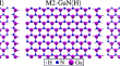
Structural and electronic properties of hydrogenated gallium nitride with vacancy and do** defects
The onset of new physical properties in two-dimensional materials has attracted great interest in technological applications. In this contribution,...
-
Deformation of Semipolar and Polar Gallium Nitride Synthesized on a Silicon Substrate
AbstractResults from studying deformation are obtained for semipolar GaN(11–22) grown on a nanostructured Si(113) substrate and polar GaN(0001) grown...

-
Performance analysis of gallium nitride-based DH-HEMT with polarization-graded AlGaN back-barrier layer
In this paper, polarization-graded AlGaN back-barrier nanolayer has been introduced to improve the DC and RF parameters of gallium nitride-based high...

-
-
Anomalously Large Burgers Vectors of Screw Dislocations in Gallium Nitride Nanowires
AbstractThe results of structural studies of GaN nanowires containing screw dislocations are presented. It is found that the length of the Burgers...

-
Optical Properties of Quasi-Bulk Gallium-Nitride Crystals with Highly Oriented Texture Structure
AbstractThe results of studying the optical properties of gallium-nitride samples with a highly oriented texture structure, grown without using a...

-
Nanomechanical Phase Shifting on a Gallium Arsenide Platform
Integrated photonics on membranes containing quantum dots constitute a promising platform for quantum information processing. On-chip photonic...
-
Boron Nitride and Its Hybrids: Synthesis, Properties and Potential Applications
Two-dimensional (2D) materials and their hybrid structures have garnered immense attention over the past two decades. The distinct properties...
-
The Structure of Domain and Antiphase Boundaries in κ-Phase of Gallium Oxide
AbstractThe results of an experimental study of the real structure of thin films of κ-phase gallium oxide are reported. It has been established by...
-
Gallium nitride wafer slicing by a sub-nanosecond laser: effect of pulse energy and laser shot spacing
Gallium nitride (GaN)-based devices surpass the traditional silicon-based power devices in terms of higher breakdown voltage, faster-switching speed,...

-
Electron Beam-Stimulated Luminescence of Helium Ion-Irradiated Hexagonal Boron Nitride
AbstractThe impact of irradiation with a focused helium ion beam and an electron beam on the cathodoluminescence (CL) of hexagonal boron nitride was...

-
Effect of tunnelling in double barrier nitride (AlGaN/GaN) heterojunction
In a double-barrier heterostructure made of (AlGaN/GaN), the tunneling effect has been investigated, and the probability that electrons will pass...

-
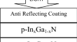
TCAD based performance assessment of Indium Gallium Nitride based single junction solar cells for different mole fractions of Indium
The tailoring the band gap energy of the ternary Indium Gallium Nitride (In x Ga (1−x) N) alloy shows a good spectral match with a range of wavelength in...
-
III-Nitride HEMTs for THz Applications
This chapter exhaustively explores the prospects of III-Nitride-based High Electron Mobility Transistors (HEMTs) for THz applications. III-Nitride...
-
Spectra of the Gallium Nitride Growth Traps
The energy spectra of growth traps in the epitaxial layers of undoped and doped gallium nitride grown under various technological conditions are...
-
Electrical Properties of a Composition Based on Polydimethylsiloxane Filled with Gallium Oxide
AbstractIn the present paper, the effect of gallium β-oxide introduced into the polydimethylsiloxane elastomer on the electrical properties of the...

-
Epitaxial growth of 2D gallium selenide flakes for strong nonlinear optical response and visible-light photodetection
As an emerging group III–VI semiconductor two-dimensional (2D) material, gallium selenide (GaSe) has attracted much attention due to its excellent...

-
The Effect of AlN Buffer Layer Morphology on the Structural Quality of a Semipolar GaN Layer Grown on a Si(001) Substrate, According to Transmission Electron Microscopy Data
AbstractStructural features of the interface between a semipolar gallium nitride layer and buffer layer of aluminum nitride grown on a SiC/Si(001)...

-
Growth of magnesium nitride thin films on various surfaces via atomic-nitrogen-assisted molecular beam epitaxy at moderate substrate temperatures
We report on the growth of Mg 3 N 2 thin films via atomic-nitrogen-assisted molecular beam epitaxy (MBE) on various surfaces, i.e ., silicon, sapphire,...
