Search
Search Results
-
Method for Determining the Etching Rate in Phosphate Glass Detectors
AbstractA method for determining the etching rate of phosphate glass irradiated with heavy ions is presented. The etching rates in the track area and...

-
Surface micro/nanostructure on the TZ30 alloy regulated by the electrochemical etching method
The Ti-30Zr-5Al-3V (TZ30) alloy, having a low elastic modulus close to biological bones, promises great application potential for implant...

-
Performance of SiQDs and H_Si nanopillars/etched Si electrical sensor synthesized by aggressive laser-assisted etching method: comparative study
In the current study, a comparative approach was followed to explore the effect of two specific forms of Si nanocrystallites structures (Si quantum...

-
High Speed Etching of Silicon in NaOH-Based Solution
In this research, the effect of hydroxylamine (NH2OH) on the etching characteristics of sodium hydroxide (NaOH) is investigated. To perform this...
-
Etching-free pixel definition in InGaN green micro-LEDs
The traditional plasma etching process for defining micro-LED pixels could lead to significant sidewall damage. Defects near sidewall regions act as...

-
Plasmachemical Etching in Postgrowth Technology of Photovoltaic Converters
AbstractInvestigation of the heterostructure plasmachemical etching technology for fabricating multi-junction photovoltaic converters has been...
-
Study of Etching Features of Quartz Glass Irradiated with Xenon Ions
AbstractThe first results of testing KU-2 optical quartz glass as a detector of accelerated heavy ions are presented. The results of etching the...
-
Study of Electrochemical Etching Surface of Ultrafine-Grained Nickel Using Scanning Tunneling Microscopy
AbstractAn approach that allows a qualitative and quantitative analysis of the grain structure of ultrafine grained nickel by electrochemical etching...

-
Ammonium Fluoride as an Inhibitor of Liquid Acid Etching of YBCO
AbstractAmong classical applications of superconductivity, various microelectronic devices are of key importance. As a rule, such devices represent a...

-
Dynamics of Deposition and Removal of a Fluorocarbon Film in the Cyclic Process of Plasma-Chemical Etching of Silicon
AbstractIn situ measurements were made of the dynamics of deposition and etching of a fluorocarbon film (FCF) during cyclic plasma-chemical etching...

-
Influence of Electromagnetic Field Power and Temperature of Inductively Coupled Plasma Etching on the Uniformity of a Patterned Sapphire Substrate
Abstract—Patterned sapphire substrate technology can improve the growth performance and luminous efficiency of light-emitting diodes. In this work,...

-
Microchannels fabrication in nanoporous silicate matrix by femtosecond direct laser writing and subsequent chemical etching
Femtosecond direct laser writing (FDLW) is a powerful tool for modification of the properties of transparent materials through nonlinear multiphoton...

-
Controlling the size and curvature radius of concave microlens array on fused silica by wet-etching-assisted with picosecond laser
In this paper, we study wet-etching-assisted with picosecond laser for the fabrication of concave MLA on fused silica. Compared with the previous...

-
Etching of “Microwire-on-Insulator”-Type Structures
AbstractNanoribbons from different materials, such as graphene and topological insulators, are currently intensively studied as structures needed in...

-
Production and characterization of porous silicon via laser-assisted etching as photodetector: effect of different HF concentrations
The effect of hydrofluoric (HF) acid concentration on the optoelectronic properties of porous silicon (PS) was investigated. The laser-assisted...

-
Laser Etching of Quasi-1D TiS3 Nanoribbons by Raman Spectrophotometer
Abstract —Quasi one-dimensional materials are technologically very important due to their extraordinary properties. The properties are enhanced when...

-
Improved Superconducting Performance of YBCO-Coated Conductors by Low Energy Density Argon Ion Etching
The a -axis grains and other secondary phase impurities, which are of great suppression for the superconducting properties, are easily formed on the...

-
Application of honeycomb pattern to Ti2AlN MAX phase films by plasma etching
The honeycomb pattern possesses a distinctive hexagonal structure capable of seamless repetition on a flat surface, leaving no gaps. Moreover, all...

-
Optical Properties of Silicon Nanowires Obtained by Metal-Assisted Chemical Etching Using Gold Nanoparticles
Owing to their unique structural and physical properties, silicon nanowires are a promising material for electronics, photovoltaics, photonics,...

-
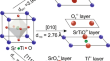
Realization of atomically flat single terminated surface of SrTiO3 (001), (110), and (111) substrate by chemical etching
The research on perovskite oxide thin films, interfaces, and super-lattices demands the need for the atomically flat surface of the substrate to...